EVALA5972D STMicroelectronics, EVALA5972D Datasheet
EVALA5972D
Specifications of EVALA5972D


Related parts for EVALA5972D


EVALA5972D Summary of contents
Page 1
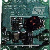
Designing with the L5972D high efficiency DC-DC converter Introduction The L5972D is a step-down monolithic power switching regulator capable of delivering output voltages from 1.235 The operating input voltage ranges from ...
Page 2
Contents Contents 1 Pin functions . . . . . . . . . . . . . . . . . . . . . . . . . . . . . . . . . . . ...
Page 3
AN1517 6.1 Positive buck-boost regulator . . . . . . . . . . . . . . . . . . . . . . . . . . . . . . . . . . 24 ...
Page 4
List of figures List of figures Figure 1. Demonstration board . . . . . . . . . . . . . . . . . . . . . . . . . . . . . . ...
Page 5
AN1517 1 Pin functions 1.1 Pin description Table 1. Pin description N. Name 1 OUT Regulator output. Ground. Lead connected directly to the frame in order to reduce the junction-to-ambient 2 GND thermal resistance. Ground. Lead connected directly to the ...
Page 6
Functional description 2 Functional description The main internal blocks are shown in the device block diagram in ● A voltage regulator that supplies the internal circuitry. From this regulator, a 3.3 V reference voltage is externally available. ● A voltage ...
Page 7
AN1517 Figure 5. Internal regulator circuit 2.3 Oscillator Figure 6 shows the block diagram of the oscillator circuit. The Clock Generator provides the switching frequency of the device, which is internally fixed at 250 kHz. The Frequency Shifter block acts ...
Page 8
Functional description Due to this reduction of the ON time, the output voltage decreases. Since the minimum switch ON time (necessary to avoid a false over-current signal) is too short to obtain a sufficiently low duty cycle at 250 kHz, ...
Page 9
AN1517 the faster the rise time, the lower the turn ON losses. However, there is a limit introduced by the recovery time of the recirculation diode. In fact, when the current of the power element is equal to the inductor ...
Page 10
Additional features and protection 3 Additional features and protection 3.1 Feedback disconnection If the feedback is disconnected, the duty cycle increases towards the maximum allowed value, bringing the output voltage close to the input supply. This condition could destroy the ...
Page 11
AN1517 4 Closing the loop Figure 9. Block diagram of the loop 4.1 Error amplifier and compensation network The output L-C filter of a step-down converter contributes with 180 degrees phase shift in the control loop. For this reason a ...
Page 12
Closing the loop Figure 10. Error amplifier equivalent circuit and compensation network The poles of this transfer function are (if C Equation 3 Equation 4 where the zero is defined as: Equation the low frequency which sets ...
Page 13
AN1517 Equation 7 The zero of this transfer function is given by: Equation the zero introduced by the ESR of the output capacitor and it is very important to 0 increase the phase margin of the loop. ...
Page 14
Closing the loop This means that even if the input voltage changes, the error amplifier does not change its value to keep the loop in regulation, thus ensuring a better line regulation and line transient response. To sum up, the ...
Page 15
AN1517 Figure 12. Phase plot The cut off frequency and the phase margin are: Equation 22.8KHz Phase margin = 39.8° C Closing the loop 15/29 ...
Page 16
Application information 5 Application information 5.1 Component selection 5.1.1 Input capacitor The input capacitor must be able to withstand the maximum input operating voltage and the maximum RMS input current. Since step-down converters draw current from the input in pulses, ...
Page 17
AN1517 5.1.2 Output capacitor The output capacitor is very important to meet the output voltage ripple requirement. Using a small inductor value is useful to reduce the size of the choke but it increases the current ripple. So, to reduce ...
Page 18
Application information Table 4. Inductor selection Manufacturer Coilcraft Coiltronics BI Epcos Wurth Elektronik 5.2 Layout considerations The layout of switching DC-DC converters is very important to minimize noise and interference. Power-generating portions of the layout are the main cause of ...
Page 19
AN1517 5.3 Thermal considerations The dissipated power of the device is tie to three different sources: ● switch losses due to the not negligible R Equation 21 where D is the duty cycle of the application. Note that the duty ...
Page 20
Application information Considering that the device in SO-8 (4+2+2) package mounted on board with a good groundplane has a thermal resistance junction to ambient (Rth considering an ambient temperature of about 70 °C. Equation 26 5.4 Short-circuit protection In over-current ...
Page 21
AN1517 Figure 14. Short-circuit current V Figure 15. Short-circuit current V In Figure 14 and increases for a given component list, the current peak increases also. The current limit is immediately triggered but the current peak increases until the current ...
Page 22
... V POSCAP 10TPB100M 100 µ C1206C221J5GAC 220 pF, 5 C1206C223K5RAC 22 nF, 10 5.6 K, 1%, 0.1 W 0603 3.3 K, 1%, 0.1 W 0603 4.7 K, 1%, 0.1 W 0603 STPS2L25U DO3316P-333 33 µH, 2.1 A 42mm AM00132v1 AM00133v1 AN1517 Manufacturer Tokin Sanyo KEMET KEMET Neohm Neohm Neohm STMicroelectronics Coilcraft 34mm ...
Page 23
AN1517 Figure 19. PCB layout (front side) Below are some graphs showing the T voltage conditions. Figure 20. Junction temperature vs. output current TJ(°C) 100.0 90.0 Vin=5V Tamb.=25 °C 80.0 70.0 60.0 50.0 40.0 30.0 20.0 0.2 0.4 0.6 0.8 ...
Page 24
Application ideas 6 Application ideas 6.1 Positive buck-boost regulator The device can be used to implement an step-up/down converter with a positive output voltage. Figure The input voltage can range from 5 V and 35 V. ...
Page 25
AN1517 7.1 Dual output voltage with auxiliary winding When two output voltages are required possible to create a dual output voltage converter by using a coupled inductor. During the ON phase the current is delivered to V while ...
Page 26
Compensation network with MLCC (multiple layer ceramic capacitor) at the output 8 Compensation network with MLCC (multiple layer ceramic capacitor) at the output MLCCs with values in the range of 10 µF-22 µF and rated voltages in the range of ...
Page 27
AN1517 Compensation network with MLCC (multiple layer ceramic capacitor) at the output Figure 28. Soft-start network example VIN=4.4V to 25V VIN=4.4V to 25V VREF VREF VREF R=4K7 R=4K7 R=4K7 C1 C1 10uF 10uF 25V 25V Css=2.7nF Css=2.7nF CERAMIC CERAMIC Vcc ...
Page 28
Revision history 9 Revision history Table 6. Document revision history Date 08-Nov-2006 28-May-2007 28/29 Revision 1 First issue – The document has been reformatted 2 – Section 4: Closing the loop – Minor text changes AN1517 Changes modified ...
Page 29
... AN1517 Information in this document is provided solely in connection with ST products. STMicroelectronics NV and its subsidiaries (“ST”) reserve the right to make changes, corrections, modifications or improvements, to this document, and the products and services described herein at any time, without notice. All ST products are sold pursuant to ST’s terms and conditions of sale. ...