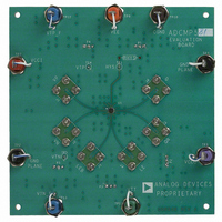
EVAL-ADCMP581BCPZ Analog Devices Inc, EVAL-ADCMP581BCPZ Datasheet

EVAL-ADCMP581BCPZ
Specifications of EVAL-ADCMP581BCPZ
Related parts for EVAL-ADCMP581BCPZ
EVAL-ADCMP581BCPZ Summary of contents
Page 1
FEATURES 180 ps propagation delay 25 ps overdrive and slew rate dispersion 8 GHz equivalent input rise time bandwidth 100 ps minimum pulse width 37 ps typical output rise/fall 10 ps deterministic jitter (DJ) 200 fs random jitter (RJ) −2 ...
Page 2
ADCMP580/ADCMP581/ADCMP582 TABLE OF CONTENTS Features .............................................................................................. 1 Applications....................................................................................... 1 Functional Block Diagram .............................................................. 1 General Description ......................................................................... 1 Revision History ............................................................................... 2 Specifications..................................................................................... 3 Timing Information ......................................................................... 5 Absolute Maximum Ratings............................................................ 6 Thermal Considerations.............................................................. 6 ESD Caution.................................................................................. 6 Pin Configurations ...
Page 3
SPECIFICATIONS −5 3 CCI EE CCO Table 1. Parameter DC INPUT CHARACTERISTICS Input Voltage Range Input Differential Range Input Offset Voltage Offset Voltage Temperature Coefficient Input Bias Current Input ...
Page 4
ADCMP580/ADCMP581/ADCMP582 Parameter ADCMP582 (PECL) Output Voltage High Level Output Voltage High Level Output Voltage High Level Output Voltage Low Level Output Voltage Low Level Output Voltage Low Level Output Voltage Differential AC PERFORMANCE Propagation Delay Propagation Delay Temperature Coefficient Propagation ...
Page 5
TIMING INFORMATION Figure 2 shows the ADCMP580/ADCMP581/ADCMP582 compare and latch timing relationships. Table 2 provides the definitions of the terms shown in Figure 2. LATCH ENABLE LATCH ENABLE DIFFERENTIAL INPUT VOLTAGE Q OUTPUT Q OUTPUT Table 2. Timing Descriptions Symbol ...
Page 6
ADCMP580/ADCMP581/ADCMP582 ABSOLUTE MAXIMUM RATINGS Table 3. Parameter SUPPLY VOLTAGES Positive Supply Voltage (V to GND) CCI Negative Supply Voltage (V to GND) EE Logic Supply Voltage (V to GND) CCO INPUT VOLTAGES Input Voltage Differential Input Voltage Input Voltage, Latch ...
Page 7
PIN CONFIGURATIONS AND FUNCTION DESCRIPTIONS PIN INDICATOR 12 GND ADCMP580 TOP VIEW GND (Not to Scale) TN Figure 3. ADCMP580 Pin Configuration Table ...
Page 8
ADCMP580/ADCMP581/ADCMP582 TYPICAL PERFORMANCE CHARACTERISTICS −5 3 CCI EE CCO COMMON-MODE BIAS SWEEP –4 –2 0 COMMON-MODE (V) Figure 6. Bias ...
Page 9
LOT2 CHAR1 RISE –3 LOT2 CHAR1 FALL LOT3 CHAR1 RISE –4 LOT3 CHAR1 FALL –5 –2 – (V) CM Figure 12. ADCMP580 Propagation Delay Error vs. Common-Mode Voltage M1 ...
Page 10
ADCMP580/ADCMP581/ADCMP582 TYPICAL APPLICATION CIRCUITS ADCMP580 LATCH INPUTS Figure 17. Zero-Crossing Detector with CML Outputs ADCMP581 LATCH INPUTS Figure ...
Page 11
APPLICATION INFORMATION POWER/GROUND LAYOUT AND BYPASSING The ADCMP58x family of comparators is designed for very high speed applications. Consequently, high speed design techniques must be used to achieve the specified performance critically important to use low impedance supply ...
Page 12
ADCMP580/ADCMP581/ADCMP582 OPTIMIZING HIGH SPEED PERFORMANCE As with any high speed comparator, proper design and layout techniques are essential to obtaining the specified performance. Stray capacitance, inductance, inductive power, and ground impedances or other layout issues can severely limit performance and ...
Page 13
COMPARATOR HYSTERESIS Adding hysteresis to a comparator is often desirable in a noisy environment or when the differential inputs are very small or slow moving. The transfer function for a comparator with hysteresis is shown in Figure 28. If the ...
Page 14
... ADCMP582BCP-RL7 −40°C to +125°C 1 ADCMP582BCPZ-WP −40°C to +125°C 1 ADCMP582BCPZ-R2 −40°C to +125°C 1 ADCMP582BCPZ-RL7 −40°C to +125°C 1 EVAL-ADCMP580BCPZ 1 EVAL-ADCMP581BCPZ 1 EVAL-ADCMP582BCPZ RoHS Compliant Part. 3.00 0.60 MAX BSC SQ 0. 2.75 TOP BSC SQ VIEW (BOTTOM VIEW ...
Page 15
NOTES ADCMP580/ADCMP581/ADCMP582 Rev Page ...
Page 16
ADCMP580/ADCMP581/ADCMP582 NOTES ©2005–2007 Analog Devices, Inc. All rights reserved. Trademarks and registered trademarks are the property of their respective owners. D04672-0-8/07(A) T Rev Page ...


