EVALB5973D STMicroelectronics, EVALB5973D Datasheet
EVALB5973D
Specifications of EVALB5973D


Related parts for EVALB5973D


EVALB5973D Summary of contents
Page 1
Designing with the 2.5 A DC-DC converter L5973D Introduction The L5973D is a step-down monolithic power switching regulator capable of delivering output voltages from 1.235 The operating input voltage ranges from ...
Page 2
Contents Contents 1 Pin functions . . . . . . . . . . . . . . . . . . . . . . . . . . . . . . . . . . . ...
Page 3
AN1518 9.5 Application circuit . . . . . . . . . . . . . . . . . . . . . . . . . . . . . . . . . . . . ...
Page 4
List of figures List of figures Figure 1. Evaluation board . . . . . . . . . . . . . . . . . . . . . . . . . . . . . . ...
Page 5
AN1518 1 Pin functions 1.1 Pin description Table 1. Pin functions N. Name 1 OUT Regulator output Master/slave synchronization. When open, a signal synchronous with the turn-OFF of the internal power is present. When connected to an external signal at ...
Page 6
Functional description 3 Functional description The main internal blocks are shown in the device block diagram in ● A voltage regulator supplying the internal circuitry. From this regulator, a 3.3 V reference voltage is externally available. ● A voltage monitor ...
Page 7
AN1518 3.3 Oscillator & synchronizer Figure 6 shows the block diagram of the oscillator circuit. The Clock Generator provides the switching frequency of the device, which is internally fixed at 250 kHz. The Frequency Shifter block acts to reduce the ...
Page 8
Functional description again. For this reason the switching frequency is also reduced, thus keeping the inductor current under its maximum threshold. The Frequency Shifter the feedback voltage. As the feedback voltage decreases (due to the reduced duty cycle), the switching ...
Page 9
AN1518 However, there is a limit introduced by the recovery time of the recirculation diode. In fact, when the current of the power element is equal to the inductor current, the diode turns OFF and the drain of the power ...
Page 10
Additional features and protection 3.8 Thermal shutdown The shutdown block generates a signal that turns OFF the power stage if the temperature of the chip goes higher than a fixed internal threshold (150 °C). The sensing element of the chip ...
Page 11
AN1518 5 Closing the loop Figure 9. Block diagram of the loop 6 Error amplifier and compensation network The output L-C filter of a step-down converter contributes with 180 degrees phase shift in the control loop. For this reason a ...
Page 12
LC filter Figure 10. Error amplifier equivalent circuit and compensation network The poles of this transfer function are (if C Equation 3 Equation 4 whereas the zero is defined as: Equation the low frequency which sets the ...
Page 13
AN1518 where R is defined as the ratio between V LOAD If R >>ESR, the previous expression of A LOAD Equation 7 The zero of this transfer function is given by: Equation the zero introduced by the ...
Page 14
PWM comparator Where K is equal to 0.076. Therefore the PWM gain is also equal to: Equation 14 This means that even if the input voltage changes, the error amplifier does not change its value to keep the loop in ...
Page 15
AN1518 Figure 12. Phase plot The cut-off frequency and the phase margin are: Equation 16 9 Application information 9.1 Component selection ● Input capacitor The input capacitor must be able to support the maximum input operating voltage and the maximum ...
Page 16
Application information and Equation 19 Where V is the freewheeling diode forward voltage and V F internal PDMOS. Considering the range D IRMS going through the input capacitor. Capacitors that can be considered are: Electrolytic capacitors: These are widely used ...
Page 17
AN1518 Table 4. Output capacitor selection Manufacturer AVX KEMET (1) Sanyo POSCAP Sprague 1. POSCAP capacitors have some characteristics which are very similar to tantalum. ● Inductor The inductor value is very important as it fixes the ripple current flowing ...
Page 18
Application information High impedance paths (in particular the feedback connections) are susceptible to interference, so they should be as far as possible from the high current paths. An layout example is provided in The input and output loops are minimized ...
Page 19
AN1518 Where T and T ON current flowing into it during the turn ON and turn OFF phases. T switching time. ● Quiescent current losses. Equation 24 Where I is the quiescent current. Q Example: – ...
Page 20
Application information 9.4 Short-circuit protection In overcurrent protection mode, when the peak current reaches the current limit, the device reduces the T ON frequency to approximately one third of its nominal value (see protection). In these conditions, the duty cycle ...
Page 21
AN1518 Figure 15. Short-circuit current V In Figure 14 and increases for a given component list, the current peak increases also. The current limit is immediately triggered but the current peak increases until the current ripple during T equal to ...
Page 22
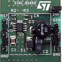
... C1206C221J5GAC 220 pF, 5 C1206C223K5RAC 22 nF, 10 5.6 kΩ , 1%, 0.1 W 0603 3.3 kΩ , 1%, 0.1 W 0603 4.7 kΩ , 1%, 0.1 W 0603 STPS2L25U DO3316P-153 15 µ L5973D EVAL.BOARD R2 R3 REF VIN GND www.st.com Description Manufacturer KEMET KEMET Neohm Neohm Neohm STMicroelectronics Coilcraft R INH SYN VOUT GND AN1518 ...
Page 23
AN1518 Figure 19. PCB layout (front side) Below, some graphs are provided which show the T and output voltage conditions, as well as some efficiency measurements. Figure 20. Junction temperature vs. output current ( Application information ...
Page 24
Application information Figure 22. Junction temperature vs. output current ( 24/30 Figure 23. Efficiency vs. output current (V = AN1518 ...
Page 25
AN1518 10 Application ideas 10.1 Positive buck-boost regulator The device can be used to implement a step-up/down converter with a positive output voltage. The figure below shows the schematic circuit of this topology for output voltage. The ...
Page 26
Application ideas Figure 25. Buck-boost regulator 10.3 Dual output voltage with auxiliary winding When two output voltages are required possible to create a dual output voltage converter by using a coupled inductor. During the ON phase, the current ...
Page 27
AN1518 Figure 27. Synchronization example 10.5 Compensation network with MLCC (multiple layer ceramic capacitor) at the output MLCCs with values in the range of 10 µF-22 µF and rated voltages in the range of 10 V-25 V are available today ...
Page 28
Application ideas 10.6 External SOFT_START network At start-up the device can quickly increase the current up to the current limit in order to charge the output capacitor. If soft ramp-up of the output voltage is required, an external soft-start network ...
Page 29
AN1518 11 Revision history Table 7. Document revision history Date 07-Sep-2003 05-Oct-2006 22-May-2007 31-Jan-2008 Revision 1 First release – New template 2 – Table 3 added 3 – Section 5: Closing the loop – Minor text changes 4 – Document ...
Page 30
... Information in this document is provided solely in connection with ST products. STMicroelectronics NV and its subsidiaries (“ST”) reserve the right to make changes, corrections, modifications or improvements, to this document, and the products and services described herein at any time, without notice. All ST products are sold pursuant to ST’s terms and conditions of sale. ...