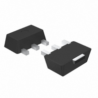
XC6372A551PR-G Torex Semiconductor Ltd, XC6372A551PR-G Datasheet

XC6372A551PR-G
Specifications of XC6372A551PR-G
XC6372A551PR
XC6372A551PR
Related parts for XC6372A551PR-G
XC6372A551PR-G Summary of contents
Page 1
XC6371/XC6372 PWM,PWM/PFM Controlled Step-up DC/DC Converters ■GENERAL DESCRIPTION The XC6371/XC6372 series is a group of PWM controlled and PWM/PFM controlled step-up DC/DC converters. The built-in 1.4Ω switching transistor type enables a step-up circuit to be configured using only three components, ...
Page 2
XC6371/XC6372 ■PIN CONFIGURATION ■PIN ASSIGNMENT XC6371/XC6372A PIN NUMBER SOT-89 USP- - XC6371/XC6372C PIN NUMBER SOT-89-5 USP- 2/17 Series *The dissipation ...
Page 3
CLASSIFICATION ●Selection Guide START PWM PWM/PFM XC6372 ●Ordering Information * XC6371①②③④⑤⑥-⑦ : PWM controlled * XC6372①②③④⑤⑥-⑦ : PWM/PFM switching control DESIGNATOR DESCRIPTION Type of ① DC/DC Converter ②③ Output Voltage ④ Oscillation Frequency Packages ⑤⑥-⑦ ...
Page 4
XC6371/XC6372 ■BLOCK DIAGRAMS XC6371/XC6372A, C (The V pin serves also as V OUT VLx l imi ter Buffer PWM Control V SS OSC 50/100/180KHz EXT Chip Enable CE Note: The CE pin is only used with ...
Page 5
CHARACTERISTICS V =5.0V, FOSC=100kHZ XC6371/72A501 OUT PARAMETER SYMBOL Output Voltage V OUT Maximum Input Voltage V IN Operation Start Voltage V ST1 Oscillation Start Voltage V ST2 No Load Input Current I IN Supply Current 1 I DD1 Supply ...
Page 6
XC6371/XC6372 ■ELECTRICAL CHARACTERISTICS (Continued) XC6371/72C501 V PARAMETER SYMBOL Output Voltage V OUT Maximum Input Voltage V IN Operation Start Voltage V ST1 Operation Start Voltage V ST2 No Load Input Current I IN Supply Current 1 I DD1 Supply Current ...
Page 7
APPRICATION CIRCUITS Circuit 1: XC6372A series L : 100μH (CR54, SUMIDA 100μH (CR54, SUMIDA MA2Q735 (Schottky Diode; MATUSHITA 16V47μF (Tantalum Capacitor, NICHICHEMI MCE) L XC6371/XC6372 Circuit 2: XC6372C series L : 100μH (CR54, ...
Page 8
XC6371/XC6372 ■TYPICAL PERFORMANCE CHARACTERISTICS (1) Output Voltage vs. Output Current XC6371A501PR =47μF(Tantalum) L=100μH(CR54),C L 5.2 1.2V 1.5V 5.1 V =0.9V IN 5.0 4.9 4.8 0 100 (mA) Output Current:I OUT XC6372A501PR L=100μH (CR54) , C =47μF (Tantalum) L ...
Page 9
PERFORMANCE CHARACTERISTICS (Continued) (2) Efficiency vs. Output Current XC6371A501PR =47μF(Tantalum) L=100μH(CR54),C L 100 =0.9V IN 1. (mA) Output Current:I OUT XC6371A301PR 100 4.0V 80 3. ...
Page 10
XC6371/XC6372 ■TYPICAL PERFORMANCE CHARACTERISTICS (Continued) (3) Ripple Voltage vs. Output Current 10/17 Series XC6371A301PR L=100μH(CR54),C 100 0.1 1 Output Current:I =47μF(Tantalum) L 1.8V 1.5V 1.2V 2.7V =0.9V 10 100 1000 1000 (mA) OUT ...
Page 11
PERFORMANCE CHARACTERISTICS (Continued) (4) No Load Input Current vs. Input Voltage XC6372A501PR L=100μH (CR54) , C =47μF (Tantalum) L 200 150 100 Input Voltage:V (V) IN XC6371A301PR L=100μH (CR54) , C 500 400 ...
Page 12
XC6371/XC6372 ■TYPICAL PERFORMANCE CHARACTERISTICS (Continued) (5) Operation Start Voltage / Hold Voltage vs. Output Current (6) Load Transient Response 12/17 Series ...
Page 13
INFORMATION ●SOT-89 ●USP-6B XC6371/XC6372 ●SOT-89-5 Series 13/17 ...
Page 14
XC6371/XC6372 ■PACKAGING INFORMATION (Continued) ●USP-6B Reference Pattern Layout 14/17 Series ●USP-6B Reference Metal Mask Design ...
Page 15
RULE [XC6371/XC6372] ●SOT-89, SOT-89 SOT-89 (TOP VIEW) SOT-89-5 (TOP VIEW) ① represents product series MARK PRODUCT SERIES A XC6371A A XC6371C ② represents integer of output voltage and oscillation frequency OUTPUT VOLTAGE (V) 50kHz 1.x B ...
Page 16
XC6371/XC6372 ■MARKING RULE (Continued) [XC6371/XC6372] (Continued) ●USP-6B USP-6B (TOP VIEW) 16/17 Series ① represents product series MARK 5 2 ② represents product classification MARK A C ③④ represents output voltage (ex.) MARK ③ ④ ⑤ represents ...
Page 17
... Should you wish to use the products under conditions exceeding the specifications, please consult us or our representatives assume no responsibility for damage or loss due to abnormal use. 7. All rights reserved. No part of this datasheet may be copied or reproduced without the prior permission of TOREX SEMICONDUCTOR LTD. XC6371/XC6372 Series 17/17 ...


