CY3210-28XXX Cypress Semiconductor Corp, CY3210-28XXX Datasheet - Page 10
CY3210-28XXX
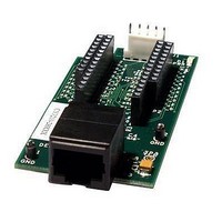
Manufacturer Part Number
CY3210-28XXX
Description
EVALUATION POD FOR CY8C28X PSOC
Manufacturer
Cypress Semiconductor Corp
Series
PSoC®r
Datasheet
1.CY3280-28XXX.pdf
(28 pages)
Specifications of CY3210-28XXX
Accessory Type
Emulation Pod
Interface Type
ICE, I2C, RS232, MiniProg,
Operating Supply Voltage
9V, 12 V
Lead Free Status / RoHS Status
Lead free / RoHS Compliant
For Use With/related Products
CY8C28 Family
Lead Free Status / RoHS Status
Lead free / RoHS Compliant, Lead free / RoHS Compliant


Quick Start
10
Table 2-1. Design Features in Universal CapSense Controller
Sensing traces are routed
through a connector to
sensors.
Sensing traces are routed
to other schematic ele-
ments.
Sensing traces are
located on the top layer.
Several regulators are
used, including a variable
regulator.
Test point on CMOD.
dGND spacing is general-
ized for noise immunity
and sensitivity.
Connection to shield elec-
trode is through a jumper
(module -J2)
Design Features
CY3280-28XXX Universal CapSense® Controller Development Kit Guide, Spec. # 001-57457 Rev. **
Buttons, sliders, and
LEDs are placed on the
module board for greater
flexibility with custom
modules for development
and subsequent releases.
Universality of the board is
enabled by population/
depopulation of 0Ω resis-
tors
Using vias to route traces
to bottom of board and
back to connector
increases parasitic capac-
itance.
To demonstrate
CapSense at several volt-
ages.
Accessibility of charge/
discharge waveforms
Universality of kit required
middle-ground on many
parameters.
Flexibility of module
boards for both CSD and
CSA control boards.
Reason for Feature
Connectors increase the
parasitic capacitance of
the sensors, effectively
reducing their sensitivity.
Connectors also create
another path for noise to
enter the system.
Solder pads of 0Ω resis-
tors increase parasitic
capacitance.
Possible noise sensitivity
to stimulus on top side of
board. Finger presses on
routing of control board
can lead to sensor activa-
tion.
Global and User Module
parameters may need to
be verified with changing
power supply.
A test point increases
noise sensitivity by acting
as an antenna.
Design is not optimized for
high noise or very thick
overlays
Higher resistance paths
can impair performance of
shield electrode in CSD
projects.
Impact
Sensors and control cir-
cuitry should be located
on the same printed circuit
board. Lower parasitic
capacitance by reducing
trace lengths.
Route traces directly to
sensing elements. Use as
few 0Ω resistors as possi-
ble.
Route sensing traces on
non-user side of printed
circuit board. Route sens-
ing traces as far from
noise sources as possible.
Supply one regulated volt-
age to PSoC.
Solder-pad test points for
leads offer better noise
immunity if test points are
required.
Increase spacing for
thicker overlays and better
sensitivity. Decrease
spacing for greater noise
immunity.
Dedicated trace for shield
electrode. Remove jump-
ers wherever possible.
Recommended Change
[+] Feedback
Related parts for CY3210-28XXX
Image
Part Number
Description
Manufacturer
Datasheet
Request
R

Part Number:
Description:
SMA RF Module For CYRF7936 CyFi Transceiver (2-pack With Antennas)
Manufacturer:
Cypress Semiconductor Corp

Part Number:
Description:
KIT EVAL PSOC EXPRESS
Manufacturer:
Cypress Semiconductor Corp
Part Number:
Description:
KIT EVAL PSOC WUSB LP
Manufacturer:
Cypress Semiconductor Corp

Part Number:
Description:
EVALUATION POD FOR CY8C29X66
Manufacturer:
Cypress Semiconductor Corp
Datasheet:
Part Number:
Description:
CyFi RF Development Kit For PSoC Devices And CyFi Transceivers
Manufacturer:
Cypress Semiconductor Corp
Part Number:
Description:
MCU, MPU & DSP Development Tools PSoC EXPRESS DEV KIT
Manufacturer:
Cypress Semiconductor Corp

Part Number:
Description:
KIT PSOC FAN MODULES
Manufacturer:
Cypress Semiconductor Corp
Datasheet:
Part Number:
Description:
KIT EVAL PSOC W/C COMPILER
Manufacturer:
Cypress Semiconductor Corp

Part Number:
Description:
KIT PSOC PROTO MODULES
Manufacturer:
Cypress Semiconductor Corp

Part Number:
Description:
EVALUATION POD FOR CY8C24X23
Manufacturer:
Cypress Semiconductor Corp
Datasheet:

Part Number:
Description:
KIT EVAL POWERLINE HIGH VOLT
Manufacturer:
Cypress Semiconductor Corp
Datasheet:

Part Number:
Description:
KIT PSOC FIRST TOUCH
Manufacturer:
Cypress Semiconductor Corp
Datasheet:

Part Number:
Description:
EVAL KIT WORLDTOUR2
Manufacturer:
Cypress Semiconductor Corp
Datasheet:

Part Number:
Description:
KIT UNIVERSAL CAPSENSE CTRLR
Manufacturer:
Cypress Semiconductor Corp
Datasheet: