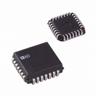
AD1555AP Analog Devices Inc, AD1555AP Datasheet - Page 20

AD1555AP
Manufacturer Part Number
AD1555AP
Description
IC,Converter, Other/Special/Miscellaneous,BICMOS,LDCC,28PIN
Manufacturer
Analog Devices Inc
Datasheet
1.AD1555APZ.pdf
(24 pages)
Specifications of AD1555AP
Rohs Status
RoHS non-compliant
Number Of Bits
24
Sampling Rate (per Second)
256k
Data Interface
Serial, Parallel
Number Of Converters
1
Power Dissipation (max)
96W
Voltage Supply Source
Dual ±
Operating Temperature
0°C ~ 85°C
Mounting Type
Surface Mount
Package / Case
28-LCC (J-Lead)
For Use With
EVAL-AD1555/56EB - BOARD EVAL FOR AD1555/56
Lead Free Status / RoHS Status
Available stocks
Company
Part Number
Manufacturer
Quantity
Price
Part Number:
AD1555AP
Manufacturer:
ADI/亚德诺
Quantity:
20 000
Company:
Part Number:
AD1555APRL
Manufacturer:
Analog Devices Inc
Quantity:
10 000
Company:
Part Number:
AD1555APZ
Manufacturer:
Analog Devices Inc
Quantity:
10 000
Company:
Part Number:
AD1555APZRL
Manufacturer:
Analog Devices Inc
Quantity:
10 000
AD1555/AD1556
RESET Operation
The RESET pin initializes the AD1556 in a known state.
RESET is active on the next CLKIN rising edge after the
RESET input is brought high as shown in Figure 4. The reset
value of each bit of the configuration and the status registers are
indicated in Table V and Table VIII. The filter memories are
not cleared by the reset. Filter convolutions begin on the next
CLKIN rising edge after the RESET input is returned low. A
RESET operation is done on power-up, independent of the
RESET pin state.
In multiple ADCs applications where absolute synchroniza-
tion—even below the noise floor—is required, RESETD, which
resets the decimator, can be tied to RESET to ensure this
synchronization.
Power-Down Operation
The PWRDN pin puts the AD1556 in a power-down state.
PWRDN is active on the next CLKIN rising edge after the
PWRDN input is brought high. While in this state, MCLK is
held at a fixed level and the AD1555 is therefore powered
down too. The serial interface remains active allowing read and
write operations of the AD1556. The configuration and status
registers maintain their content during the power-down state.
SYNC Operation
SYNC is used to create a relationship between the analog input
signal and the output samples of the AD1556. The SYNC event
does two things:
•
•
Bit
Number
DB15 (MSB)
DB14
DB13
DB12
DB11
DB10
DB9
DB8
DB7
DB6
DB5
DB4
DB3
DB2
DB1
DB0 (LSB)
It synchronizes the AD1555 clock, MCLK, to the AD1556
clock, CLKIN, as shown in Figure 3.
It clears the filter and then initiates the filter convolution.
Exactly one sampling rate delay later, the DRDY pin goes
high. A SYNC event occurs on the next CLKIN rising edge
after the SYNC input is brought high as shown in Figure 3.
The DRDY output goes high on the next falling edge of
CLKIN. SYNC may be applied once or kept high, or applied
synchronously at the output word rate, all with the same effect.
Name
X
X
X
X
PWRDN
CSEL
X
BW2
BW1
BW0
DRDYBUF
CB4
CB3
CB2
CB1
CB0
Table V. Configuration Register Data Bits
–20–
Configuring and Interfacing the AD1556
The AD1556 configuration can be loaded either by hardware
(H/S pin high) or via the serial interface of the AD1556 (H/S
pin low). To operate with the AD1556, the CLKIN clock must be
kept running at the nominal frequency of 1.024 MHz. Table V
gives the description of each bit of the configuration register and
Table VI defines the selection of the filter bandwidth. When the
software mode is selected (H/S pin low), the configuration register
is loaded using the pins DIN, SCLK, CS, and R/W. In this mode,
when RESET is active, the configuration register mimics the selec-
tion of the hardware pins. The AD1556 and the AD1555 can be
put in power-down by software.
The DRDYBUF bit controls the operating mode of the DRDY
output pin. When the DRDYBUF bit is low, the DRDY is a con-
ventional CMOS push-pull output buffer as shown in Figure 11.
When the DRDYBUF bit is high, the DRDY output pin is an
open drain PMOS pull-up as shown in Figure 11. Many DRDY
pins may be connected with an external pull-down resistor in a
wired OR to minimize the interconnection between the AD1556s
and the microprocessor in multichannel applications. The DRDY
pin is protected against bit contention.
By connecting DRDY to RSEL directly, and applying 48 SCLK
cycles, both data and status can be read sequentially, data
register first.
BW2
0
0
0
0
1
1
1
1
Description
Power-Down Mode
Select TDATA Input
Filter Bandwidth Selection
Filter Bandwidth Selection
Filter Bandwidth Selection
DRDY Output Mode
PGA Input Select
PGA Input Select
PGA Gain Select
PGA Gain Select
PGA Gain Select
Table VI. Filter Bandwidth Selection
BW1
0
0
1
1
0
0
1
1
BW0
0
1
0
1
0
1
0
1
Output Rate (ms)
4
2
1
1/2
1/4
1/8
1/16
Reserved
RESET State
X
X
X
X
PWRDN
CSEL
X
BW2
BW1
BW0
0 (Push-Pull)
PGA4
PGA3
PGA2
PGA1
PGA0
REV. B


