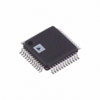
AD1833AASTZ Analog Devices Inc, AD1833AASTZ Datasheet - Page 13

AD1833AASTZ
Manufacturer Part Number
AD1833AASTZ
Description
6 Channel 24 Bit 192 KHz DAC I.C.
Manufacturer
Analog Devices Inc
Datasheet
1.AD1833ACSTZ.pdf
(20 pages)
Specifications of AD1833AASTZ
Number Of Bits
24
Data Interface
DSP, I²S, Serial
Number Of Converters
6
Voltage Supply Source
Analog and Digital
Operating Temperature
-40°C ~ 85°C
Mounting Type
Surface Mount
Package / Case
48-LQFP
Lead Free Status / RoHS Status
Lead free / RoHS Compliant
Power Dissipation (max)
-
Settling Time
-
Lead Free Status / RoHS Status
Lead free / RoHS Compliant
Available stocks
Company
Part Number
Manufacturer
Quantity
Price
Company:
Part Number:
AD1833AASTZ
Manufacturer:
Analog Devices Inc
Quantity:
10 000
Company:
Part Number:
AD1833AASTZ-REEL
Manufacturer:
Analog Devices Inc
Quantity:
10 000
MCLK Select
The AD1833A allows the matching of available external MCLK
frequencies to the required internal MCLK rate. The MCLK
modification factor can be selected from 2, 1, or
Bit 4 and Bit 3 of Control Register 3. Internally, the AD1833A
requires an MCLK of 24.576 MHz for sample rates of 48 kHz,
96 kHz, and 192 kHz. In the case of 48 kHz data with an
MCLK of 256
MCLK of 768
followed by a clock doubler. With an MCLK of 512
MCLK is passed through unmodified (see Table XII).
Bit 4
0
0
1
1
Channel Zero Status
The AD1833A provides individual logic output status indicators
when zero data is sent to a channel for 1024 or more consecutive
sample periods in all modes except right-justified. There is also
REV. 0
Sampling Rate
f
32
64
128
44.1
88.2
176.4
48
96
192
S
(kHz)
Bit 3
0
1
0
1
f
f
S
S
Table XII. MCLK Settings
, a divide-by-3 block ( 3) is first implemented
, a clock doubler is used, whereas with an
Interpolator Mode
Required
8
4
2
8
4
2
8
4
2
*Must be programmed to zero.
Address
15–12
0 0 1
0 0 1
0 1 0
0 1 0
0 1 1
0 1 1
Modification Factor
MCLK
MCLK
MCLK
Reserved
0
1
0
1
0
1
2 Internally
1 Internally
2
/
3
Internally
Table XIV. MCLK vs. Sample Rate Selection
Internal MCLK
Required (MHz)
16.384
22.5792
24.576
Reserved*
11
0
Table XV. Volume Control Registers
2
/
3
by writing to
f
S
10
0
, the
–13–
Volume Control
9–0
Channel 1 Volume Control (OUTL1)
Channel 2 Volume Control (OUTR1)
Channel 3 Volume Control (OUTL2)
Channel 4 Volume Control (OUTR2)
Channel 5 Volume Control (OUTL3)
Channel 6 Volume Control (OUTR3)
a global zero flag that indicates all channels contain zero data.
The polarity of the zero signal is programmable by writing to
Control Bit 2 (see Table XIII). In right-justified mode, the six
individual channel flags are best used as three stereo zero flags
by combining pairs of them through suitable logic gates. Then,
when both the left and right inputs are zero for 1024 clock cycles,
i.e., a stereo zero input for 1024 sample periods, the combined
result of the two individual flags will become active, indicat-
ing a stereo zero.
DAC Volume Control Registers
The AD1833A has six volume control registers, one for each of
the six DAC channels. Volume control is exercised by writing to
the relevant register associated with each DAC. This setting is
used to attenuate the DAC output. Full-scale setting (all 1s) is
equivalent to zero attenuation (see Table XV).
Suitable External MCLK Frequencies (MHz)
MCLK
8192
11.2896
12.288
2
Bit 2
0
1
Table XIII. Zero Detect
MCLK
16.384
22.5792
24.576
Channel Zero Status
Active High
Active Low
1
MCLK
24.576
33.8688
36.864
AD1833A
2
/
3


