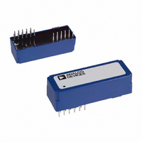
a
GENERAL DESCRIPTION
The AD260 is designed using Analog Devices new IsoLogic
circuit architecture to isolate five digital control signals to/
from a microcontroller and its related field I/O components. Six
models allow all I/O combinations from five input lines to five
output lines, including combinations in between. Every AD260
effectively replaces up to five opto-isolators while also providing
the 1.5 W transformer for a 3.5 kV isolated dc-dc power supply
circuit.
Each line of the AD260 has a bandwidth of 20 MHz (min) with
a propagation delay of only 14 ns, which allows for extremely
fast data transmission. Output waveform symmetry is maintained
to within 1 ns of the input so the AD260 can be used to accu-
rately isolate time-based PWM signals.
All field or system output pins of the AD260 can be set to a high
resistance three-state level by use of the two enable pins. A field
output three-stated offers a convenient method of presetting
logic levels at power-up by use of pull-up/down resistors. Sys-
tem side outputs being three-stated allows for easy multiplexing
of multiple AD260s.
The isolation barrier of the AD260 B Grade is 100% tested at
3.5 kV rms (system to field). The barrier design also provides
excellent common-mode transient immunity from 10 kV/ s
common-mode voltage excursions of field side terminals relative
to the system side, with no false output triggering on either side.
Each output is updated within nanoseconds by input logic tran-
sitions, the AD260 also has a continuous output update feature
that automatically updates each output based on the dc level of
IsoLogic is a trademark of Analog Devices, Inc.
REV. 0
Information furnished by Analog Devices is believed to be accurate and
reliable. However, no responsibility is assumed by Analog Devices for its
use, nor for any infringements of patents or other rights of third parties
which may result from its use. No license is granted by implication or
otherwise under any patent or patent rights of Analog Devices.
FEATURES
IsoLogic™ Circuit Architecture
Isolation Test Voltage: To 3.5 kV rms
Five Isolated Logic Lines: Available in Six I/O Configurations
Logic Signal Bandwidth: 20 MHz (Min), 40 mbps (NRZ)
Isolated Power Transformer: 37 V p-p, 1.5 W Max
CMV Transient Immunity: 10 kV/ s Min
Waveform Edge Transmission Symmetry:
Field and System Output Enable/Three-State Functions
Performance Rated Over –25 C to +85 C
UL1950, IEC950, EN60950 Certification, Pending
APPLICATIONS
PLC/DCS Analog Input and Output Cards
Communications Bus Isolation
General Data Acquisition Applications
IGBT Motor Drive Controls
High Speed Digital I/O Ports
1 ns
the input. This guarantees the output is always valid 10 s after
a fault condition or after the power-up reset interval.
The AD260 also has an integral center tap transformer for gen-
erating isolated power. Typically driven by a 5 V push-pull drive
at the primary, it will generate a 37 V p-p output capable of
supplying up to 1.5 W. This can then be regulated to the de-
sired voltage, including 5 V dc for circuit components and
24 V for a 20 mA loop supply when needed.
PRODUCT HIGHLIGHTS
Six Isolated Logic Line I/O Configurations Available: The
AD260 is available in six pin-compatible versions of I/O con-
figurations to meet a wide variety of requirements.
Wide Bandwidth with Minimal Edge Error: The AD260 with
IsoLogic affords extremely fast isolation of logic signals due to its
20 MHz bandwidth and 14 ns propagation delay. It maintains a
waveform input-to-output edge transition error of typically less
than 1 ns (total) for positive vs. negative transition.
3.5 kV rms Test Voltage Isolation Rating: The AD260
B Grade is rated to operate at 1.25 kV rms and is 100% pro-
duction tested at 3.5 kV rms, using a standard ADI test method.
High Transient Immunity: The AD260 rejects common-
mode transients slewing at up to 10 kV/ s without false trigger-
ing or damage to the device.
One Technology Way, P.O. Box 9106, Norwood, MA 02062-9106, U.S.A.
Tel: 781/329-4700
Fax: 781/326-8703
ENABLE
PWRCT
5V RTN
PWRB
+5Vdc
PWRA
FLD
FLD
FLD
FLD
FLD
FLD
F3
F4
F0
F1
F2
High Speed, Logic Isolator
19
18
20
21
22
17
16
15
14
13
12
FUNCTIONAL BLOCK DIAGRAM
17V p-p OUT
CT OUT
17V p-p OUT
+5Vdc
5Vdc RTN
AD260
with Power Transformer
FIELD
World Wide Web Site: http://www.analog.com
D
D
E
E
LATCH
LATCH
LINE 1
LINE 2
LINE 0
LINE 3
LINE 4
© Analog Devices, Inc., 1998
LATCH
LATCH
LATCH
SYSTEM
D
E
D
E
D
E
5Vdc RTN
DRIVE
DRIVE
+5Vdc
AD260
+5V
(Continued on page 6)
10
11
1
2
3
4
5
6
7
8
9
S1
S2
S4
S0
S3
ENABLE
+5Vdc
5V RTN
DRVA
DRVCT
DRVB
SYS
SYS
SYS