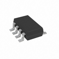
AD5227BUJZ10-RL7 Analog Devices Inc, AD5227BUJZ10-RL7 Datasheet - Page 4

AD5227BUJZ10-RL7
Manufacturer Part Number
AD5227BUJZ10-RL7
Description
IC,Digital Potentiometer,TSSOP,8PIN,PLASTIC
Manufacturer
Analog Devices Inc
Datasheet
1.AD5227BUJZ10-RL7.pdf
(16 pages)
Specifications of AD5227BUJZ10-RL7
Taps
64
Resistance (ohms)
10K
Number Of Circuits
1
Temperature Coefficient
35 ppm/°C Typical
Memory Type
Volatile
Interface
Up/Down Counter
Voltage - Supply
2.7 V ~ 5.5 V
Operating Temperature
-40°C ~ 105°C
Mounting Type
Surface Mount
Package / Case
TSOT-23-8, TSOT-8
Resistance In Ohms
10K
Lead Free Status / RoHS Status
Lead free / RoHS Compliant
Other names
AD5227BUJZ10RL7TR
Available stocks
Company
Part Number
Manufacturer
Quantity
Price
Company:
Part Number:
AD5227BUJZ10-RL7
Manufacturer:
AVX
Quantity:
34 000
Company:
Part Number:
AD5227BUJZ10-RL7
Manufacturer:
LTC
Quantity:
892
Part Number:
AD5227BUJZ10-RL7
Manufacturer:
ADI/亚德诺
Quantity:
20 000
AD5227
Parameter
INTERFACE TIMING CHARACTERISTICS (applies to all parts
1
2
3
4
5
6
7
8
9
10
INTERFACE TIMING DIAGRAMS
positions. R-DNL measures the relative step change from ideal between successive tap positions. Parts are guaranteed monotonic.
bandwidth. The highest R value results in the minimum overall power consumption.
V
Typicals represent average readings at 25°C, V
Resistor position nonlinearity error, R-INL, is the deviation from an ideal value measured between the maximum resistance and the minimum resistance wiper
NL and DNL are measured at V
DNL specification limits of ±1 LSB maximum are guaranteed monotonic operating conditions.
Resistor Terminals A, B, W have no limitations on polarity with respect to each other.
Guaranteed by design and not subject to production test.
P
Bandwidth, noise, and settling time are dependent on the terminal resistance value chosen. The lowest R value results in the fastest settling time and highest
All dynamic characteristics use V
All input control voltages are specified with t
DD
DISS
Clock Frequency
Input Clock Pulse Width
CS to CLK Setup Time
CS Rise to CLK Hold Time
U/D to Clock Fall Setup Time
= 5 V.
is calculated from (I
DD
× V
DD
W
). CMOS logic level inputs result in minimum power dissipation.
with the RDAC configured as a potentiometer divider similar to a voltage output D/A converter. V
DD
= V.
R
R
CLK
DD
U/D
CS = LOW
U/D = HIGH
= t
CS = LOW
U/D = 0
R
CLK
CS
WB
CLK
R
WB
= 5 V.
WB
F
Figure 4. Detailed Timing Diagram (Only R
1
0
1
0
1
0
= 1 ns (10% to 90% of V
t
t
UDS
CSS
Symbol
f
t
t
t
t
CLK
CH
CSS
CSH
UDS
, t
CL
t
CL
t
S
6, 10
Figure 3. Decrement R
Figure 2. Increment R
)
t
Rev. B | Page 4 of 16
CH
DD
) and timed from a voltage level of 1.6 V. Switching characteristics are measured using
Conditions
Clock level high or low
WB
WB
WB
Decrement Shown)
t
CSH
Min
10
10
10
10
Typ
A
= V
1
DD
and V
Max
50
B
= 0 V.
Unit
MHz
ns
ns
ns
ns


