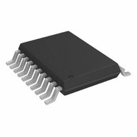
AD5254BRUZ10-RL7 Analog Devices Inc, AD5254BRUZ10-RL7 Datasheet - Page 4

AD5254BRUZ10-RL7
Manufacturer Part Number
AD5254BRUZ10-RL7
Description
IC,Digital Potentiometer,CMOS,TSSOP,20PIN,PLASTIC
Manufacturer
Analog Devices Inc
Datasheet
1.AD5254BRUZ100.pdf
(32 pages)
Specifications of AD5254BRUZ10-RL7
Taps
256
Resistance (ohms)
10K
Number Of Circuits
4
Temperature Coefficient
650 ppm/°C Typical
Memory Type
Non-Volatile
Interface
I²C, 2-Wire Serial
Voltage - Supply
2.7 V ~ 5.5 V, ±2.25 V ~ 2.75 V
Operating Temperature
-40°C ~ 85°C
Mounting Type
Surface Mount
Package / Case
20-TSSOP
Resistance In Ohms
10K
Number Of Elements
4
# Of Taps
256
Resistance (max)
10KOhm
Power Supply Requirement
Single/Dual
Interface Type
Serial (2-Wire/I2C)
Single Supply Voltage (typ)
3/5V
Dual Supply Voltage (typ)
±2.5V
Single Supply Voltage (min)
2.7V
Single Supply Voltage (max)
5.5V
Dual Supply Voltage (min)
±2.25V
Dual Supply Voltage (max)
±2.75V
Operating Temp Range
-40C to 85C
Operating Temperature Classification
Industrial
Mounting
Surface Mount
Pin Count
20
Lead Free Status / RoHS Status
Lead free / RoHS Compliant
For Use With
AD5254EVAL - BOARD EVAL FOR AD5254
Lead Free Status / Rohs Status
Compliant
Other names
AD5254BRUZ10-RL7
AD5254BRUZ10-RL7TR
AD5254BRUZ10-RL7TR
Available stocks
Company
Part Number
Manufacturer
Quantity
Price
Company:
Part Number:
AD5254BRUZ10-RL7
Manufacturer:
INFINEON
Quantity:
31 550
AD5253/AD5254
Parameter
DIGITAL INPUTS AND OUTPUTS
POWER SUPPLIES
DYNAMIC CHARACTERISTICS
1
2
3
4
5
6
7
8
Typical values represent average readings at 25°C and V
Resistor position nonlinearity error (R-INL) is the deviation from an ideal value measured between the maximum and minimum resistance wiper positions. R-DNL is the
relative step change from an ideal value measured between successive tap positions. Parts are guaranteed monotonic, except R-DNL of AD5254 1 kΩ version at V
I
INL and DNL are measured at V
DNL specification limits of ±1 LSB maximum are guaranteed monotonic operating conditions.
Resistor Terminal A, Terminal B, and Terminal W have no limitations on polarity with respect to each other.
Guaranteed by design and not subject to production test.
Command 0 NOP should be activated after Command 1 to minimize I
P
All dynamic characteristics use V
W
DISS
Input Logic High
Input Logic Low
Output Logic High (SDA)
Output Logic Low (SDA)
WP Leakage Current
A0 Leakage Current
Input Leakage Current
Input Capacitance
Single-Supply Power Range
Dual-Supply Power Range
Positive Supply Current
Negative Supply Current
EEMEM Data Storing Mode Current
EEMEM Data Restoring Mode
Power Dissipation
Power Supply Sensitivity
Bandwidth –3 dB
Total Harmonic Distortion
V
Resistor Noise Voltage
Digital Crosstalk
Analog Coupling
= V
W
is calculated from I
(Other than WP and A0)
Current
Settling Time
DD
/R for both V
6
DD
= 3 V and V
DD
7
5
× V
DD
W
= 5 V.
DD
with the RDAC configured as a potentiometer divider similar to a voltage output digital-to-analog converter. V
5, 8
DD
= 5 V.
= 5 V.
Symbol
THD
V
V
V
V
I
I
I
C
V
V
I
I
I
I
P
PSS
BW
t
e
C
C
WP
A0
I
DD
SS
DD_STORE
DD_RESTORE
S
N_WB
IH
IL
OH
OL
I
DD
DD
DISS
T
AT
/V
SS
DD
= 5 V.
DD_RESTORE
Conditions
V
V
V
V
R
R
WP = V
A0 = GND
V
V
V
V
V
V
V
V
ΔV
ΔV
R
V
V
R
(thermal noise only)
V
adjacent RDAC making full-scale
change
Signal input at A0 and measure the
output at W1, f = 1 kHz
Rev. B | Page 4 of 32
DD
DD
DD
DD
PULL-UP
PULL-UP
IN
SS
IH
IH
SS
IH
IH
IH
AB
A
A
WB
A
=1 V rms, V
= V
= V
DD
DD
= 0 V or V
= V
= V
= V
= V
= V
/V
/V
= 0 V
= –2.5 V
= 1 kΩ
= 5 V, V
= 5 V, V
= 500 Ω, f = 1 kHz
current consumption.
= 5 V ± 10%
= 3 V ± 10%
SS
SS
DD
DD
DD
DD
DD
DD
DD
= 2.2 kΩ to V
= 2.2 kΩ to V
DD
= +2.7 V/0 V or V
= +2.7 V/0 V or V
, V
, V
or V
or V
or V
or V
= 5 V or V
B
B
SS
SS
= 0 V
= 0 V, measure V
DD
IL
IL
IL
IL
= 0 V
= 0 V
B
= GND
= GND, V
= GND
= GND
= 0 V, f = 1 kHz
IL
DD
DD
= GND
= 5 V, V
= 5 V, V
DD
DD
DD
= 2.5 V,
/V
/V
W
SS
SS
SS
SS
with
= ±2.5 V
= ±2.5 V
= 0 V
= 0 V
Min
2.4
2.1
4.9
2.7
±2.25
−0.025
–0.04
Typ
5
5
–5
35
2.5
+0.010
+0.02
4
0.05
0.2
3
–80
–72
1
A
= V
Max
0.8
0.6
0.4
5
3
±1
5.5
±2.75
15
–15
0.075
+0.025
+0.04
DD
and V
B
DD
= 0 V.
Unit
V
V
V
V
V
V
μA
μA
μA
pF
V
V
μA
μA
mA
mA
mW
%/%
%/%
MHz
%
μs
nV/√Hz
dB
dB
= 2.7 V,


