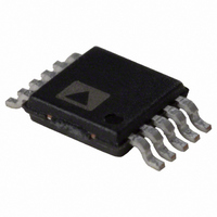
AD5314BRM Analog Devices Inc, AD5314BRM Datasheet - Page 16

AD5314BRM
Manufacturer Part Number
AD5314BRM
Description
D/A Converter (D-A) IC
Manufacturer
Analog Devices Inc
Datasheet
1.AD5304ARMZ-REEL7.pdf
(24 pages)
Specifications of AD5314BRM
Digital Ic Case Style
MSOP
No. Of Pins
10
Operating Temperature Range
-40°C To +105°C
Peak Reflow Compatible (260 C)
No
No. Of Bits
10 Bit
Leaded Process Compatible
No
Mounting Type
Surface Mount
Rohs Status
RoHS non-compliant
Settling Time
6µs
Number Of Bits
10
Data Interface
Serial
Number Of Converters
4
Voltage Supply Source
Single Supply
Power Dissipation (max)
5mW
Operating Temperature
-40°C ~ 105°C
Package / Case
10-MSOP, Micro10™, 10-uMAX, 10-uSOP
Lead Free Status / RoHS Status
Contains lead / RoHS non-compliant
Available stocks
Company
Part Number
Manufacturer
Quantity
Price
Company:
Part Number:
AD5314BRM
Manufacturer:
AD
Quantity:
5 321
Part Number:
AD5314BRM
Manufacturer:
ADI/亚德诺
Quantity:
20 000
Company:
Part Number:
AD5314BRM-REEL7
Manufacturer:
AD
Quantity:
5 510
Company:
Part Number:
AD5314BRM-REEL7
Manufacturer:
HALO
Quantity:
5 510
Part Number:
AD5314BRM/D6B
Manufacturer:
ADI/亚德诺
Quantity:
20 000
Part Number:
AD5314BRMZ
Manufacturer:
ADI/亚德诺
Quantity:
20 000
Part Number:
AD5314BRMZ-REEL
Manufacturer:
ADI/亚德诺
Quantity:
20 000
Part Number:
AD5314BRMZ-REEL7
Manufacturer:
ADI/亚德诺
Quantity:
20 000
AD5304/AD5314/AD5324
Double-Buffered Interface
The AD5304/AD5314/AD5324 DACs have double-buffered inter-
faces consisting of two banks of registers—input registers and
DAC registers. The input register is directly connected to the
input shift register and the digital code is transferred to the rele-
vant input register on completion of a valid write sequence. The
DAC register contains the digital code used by the resistor string.
Access to the DAC register is controlled by the LDAC bit. When
the LDAC bit is set high, the DAC register is latched and hence
the input register can change state without affecting the contents of
the DAC register. However, when the LDAC bit is set low, all DAC
registers are updated after a complete write sequence.
This is useful if the user requires simultaneous updating of all
DAC outputs. The user can write to three of the input registers
individually and then, by setting the LDAC bit low when writing
to the remaining DAC input register, all outputs update simult-
aneously.
These parts contain an extra feature whereby the DAC register
is not updated unless its input register has been updated since
the last time that LDAC was brought low. Normally, when LDAC
is brought low, the DAC registers are filled with the contents of
the input registers. In the case of the AD5304/AD5314/AD5324,
the part updates the DAC register only if the input register has
been changed since the last time the DAC register was updated,
thereby removing unnecessary digital crosstalk.
POWER-DOWN MODE
The AD5304/AD5314/AD5324 have low power consumption,
dissipating only 1.5 mW with a 3 V supply and 3 mW with a
5 V supply. Power consumption can be further reduced when
the DACs are not in use by putting them into power-down mode,
selected by a 0 on Bit 13 ( PD ) of the control word.
When the PD bit is set to 1, all DACs work normally with a typ-
ical power consumption of 600 μA at 5 V (500 μA at 3 V). However,
in power-down mode, the supply current falls to 200 nA at 5 V
(80 nA at 3 V) when all DACs are powered down. Not only does
the supply current drop, but also the output stage is internally
switched from the output of the amplifier, making it open-circuit.
This has the advantage that the output is three-stated while
the part is in power-down mode, and provides a defined input
condition for whatever is connected to the output of the DAC
amplifier. The output stage is illustrated in Figure 35.
Rev. F | Page 16 of 24
The bias generator, the output amplifier, the resistor string, and
all other associated linear circuitry are shut down when the power-
down mode is activated. However, the contents of the registers
are unaffected when in power-down. The time to exit power-
down is typically 2.5 μs for V
This is the time from the falling edge of the 16
when the output voltage deviates from its power down voltage.
See Figure 22 for a plot.
MICROPROCESSOR INTERFACING
AD5304/AD5314/AD5324 to ADSP-21xx
Figure 36 shows a serial interface between the AD5304/AD5314/
AD5324 and the ADSP-21xx family. The ADSP-21xx is set up
to operate in the SPORT transmit alternate framing mode. The
ADSP-21xx sport is programmed through the SPORT control
register and must be configured as follows: internal clock oper-
ation, active-low framing, and 16-bit word length. Transmission
is initiated by writing a word to the Tx register after the SPORT
has been enabled. The data is clocked out on each rising edge of
the DSP’s serial clock and clocked into the AD5304/AD5314/
AD5324 on the falling edge of the DAC’s SCLK.
Figure 36. AD5304/AD5314/AD5324 to ADSP-21xx Interface
*ADDITIONAL PINS OMITTED FOR CLARITY.
STRING DAC
RESISTOR
ADSP-21xx*
Figure 35. Output Stage during Power-Down
SCLK
POWER-DOWN
TFS
DT
CIRCUITRY
AMPLIFIER
DD
= 5 V and 5 μs when V
SYNC
DIN
SCLK
AD5324*
AD5304/
AD5314/
th
V
OUT
SCLK pulse to
DD
= 3 V.


