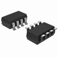
AD5662BRJ-2500RL7 Analog Devices Inc, AD5662BRJ-2500RL7 Datasheet - Page 14

AD5662BRJ-2500RL7
Manufacturer Part Number
AD5662BRJ-2500RL7
Description
IC,D/A CONVERTER,SINGLE,16-BIT,CMOS,TSSOP,8PIN
Manufacturer
Analog Devices Inc
Series
nanoDAC™r
Datasheet
1.AD5662BRJZ-2REEL7.pdf
(24 pages)
Specifications of AD5662BRJ-2500RL7
Design Resources
4 mA to 20 mA Process Control Loop Using AD5662 (CN0009) 16-Bit Fully Isolated Voltage Output Module Using AD5662, ADuM1401, and External Amplifiers (CN0063) 16-Bit Fully Isolated 4 mA to 20 mA Output Module Using AD5662, ADuM1401, and External Amplifiers (CN0064)
Settling Time
8µs
Number Of Bits
16
Data Interface
DSP, MICROWIRE™, QSPI™, Serial, SPI™
Number Of Converters
1
Voltage Supply Source
Single Supply
Power Dissipation (max)
750µW
Operating Temperature
-40°C ~ 125°C
Mounting Type
Surface Mount
Package / Case
SOT-23-8
Lead Free Status / RoHS Status
Contains lead / RoHS non-compliant
AD5662
THEORY OF OPERATION
DAC SECTION
The AD5662 DAC is fabricated on a CMOS process. The
architecture consists of a string DAC followed by an output
buffer amplifier. Figure 32 shows a block diagram of the DAC
architecture.
Since the input coding to the DAC is straight binary, the ideal
output voltage is given by
where D is the decimal equivalent of the binary code that is
loaded to the DAC register. It can range from 0 to 65,535.
RESISTOR STRING
The resistor string section is shown in Figure 33. It is simply a
string of resistors, each of value R. The code loaded to the DAC
register determines at which node on the string the voltage is
tapped off to be fed into the output amplifier. The voltage is
tapped off by closing one of the switches connecting the string
to the amplifier. Because it is a string of resistors, it is guaranteed
monotonic.
DAC REGISTER
V
OUT
=
V
R
REF
R
R
R
R
×
⎛
⎜
⎝
Figure 32. DAC Architecture
65,536
Figure 33. Resistor String
D
⎞
⎟
⎠
RESISTOR
STRING
REF (+)
REF (–)
GND
V
DD
TO OUTPUT
AMPLIFIER
R
AMPLIFIER
OUTPUT
R
V
V
FB
OUT
Rev. A | Page 14 of 24
OUTPUT AMPLIFIER
The output buffer amplifier can generate rail-to-rail voltages on
its output, which gives an output range of 0 V to V
buffer amplifier has a gain of 2 derived from a 50 kΩ resistor
divider network in the feedback path. The output amplifier’s
inverting input is available to the user, allowing for remote
sensing. This V
operation. It can drive a load of 2 kΩ in parallel with 1000 pF to
GND. The source and sink capabilities of the output amplifier can
be seen in Figure 15. The slew rate is 1.5 V/μs with a ¼ to ¾
full-scale settling time of 10 μs.
SERIAL INTERFACE
The AD5662 has a 3-wire serial interface ( SYNC , SCLK, and
DIN) that is compatible with SPI, QSPI, and MICROWIRE
interface standards as well as with most DSPs. See
a timing diagram of a typical write sequence.
The write sequence begins by bringing the SYNC line low. Data
from the DIN line is clocked into the 24-bit shift register on the
falling edge of SCLK. The serial clock frequency can be as high
as 30 MHz, making the AD5662 compatible with high speed
DSPs. On the 24
in and the programmed function is executed, that is, a change
in DAC register contents and/or a change in the mode of opera-
tion. At this stage, the SYNC line can be kept low or be brought
high. In either case, it must be brought high for a minimum of
33 ns before the next write sequence so that a falling edge of
SYNC can initiate the next write sequence. Since the SYNC
buffer draws more current when V
V
for even lower power operation. As mentioned previously it
must, however, be brought high again just before the next write
sequence.
IN
= 0.8 V, SYNC should be idled low between write sequences
FB
th
pin must be connected to V
falling clock edge, the last data bit is clocked
IN
= 2.4 V than it does when
OUT
DD
for normal
Figure 2
. This output
for


