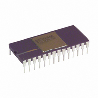
AD569BD Analog Devices Inc, AD569BD Datasheet - Page 3

AD569BD
Manufacturer Part Number
AD569BD
Description
IC,D/A CONVERTER,SINGLE,16-BIT,BICMOS,DIP,28PIN
Manufacturer
Analog Devices Inc
Datasheet
1.AD569JNZ.pdf
(12 pages)
Specifications of AD569BD
Rohs Status
RoHS non-compliant
Settling Time
4µs
Number Of Bits
16
Data Interface
Parallel
Number Of Converters
1
Voltage Supply Source
Dual ±
Operating Temperature
-25°C ~ 85°C
Mounting Type
Through Hole
Package / Case
28-CDIP (0.600", 15.24mm)
Power Dissipation (max)
-
Lead Free Status / RoHS Status
Available stocks
Company
Part Number
Manufacturer
Quantity
Price
AC PERFORMANCE CHARACTERISTICS
These characteristics are included for Design Guidance Only and are not subject to test.
+V
Parameter
Output Voltage Settling
Digital-to-Analog Glitch
Multiplying Feedthrough
Output Noise Voltage
TIMING CHARACTERISTICS
Parameter
Case A
t
t
t
Case B
t
t
t
t
t
t
Case C
t
t
t
t
t
REV. A
WC
SC
HC
WB
SB
HB
SCS
HCS
WD
WB
SB
HB
SCS
HCS
(Time to 0.001% FS
For FS Step)
Impulse
Density (1 kHz-1 MHz)
S
= +12 V; –V
Figure 1. AD569 Timing Diagram – Case A
S
= –12 V; +V
Limit
120
60
20
70
80
20
120
10
120
120
80
20
120
10
REF
= +5 V; –V
Units
ns min
ns min
ns min
ns min
ns min
ns min
ns min
ns min
ns min
ns min
ns min
ns min
ns min
ns min
Limit
5
3
6
4
500
–100
40
REF
(+V
= –5 V excepts where stated.
S
Test Conditions/Comments
150 ns Pulse on HBE, LBE, and LDAC
T
CS Pulse Width
CS Data Setup Time
CS Data Hold Time
None
HBE, LBE Pulse Width
HBE, LBE Data Setup Time
HBE, LBE Data Hold Time
CS Setup Time
CS Hold Time
LDAC Pulse Width
None
HBE, LBE Pulse Width
HBE, LBE Data Setup Time
HBE, LBE Data Hold Time
CS Setup Time
CS Hold Time
= +12 V, –V
HS
Units
nV-sec typ
dB max
nV/ Hz typ
= 140 ns min, T
s max
s typ
s max
s typ
S
= –12 V, V
–3–
HH
Test Conditions/Comments
No Load Applied
V
Measured with V
with input codes of 8000
transition). Load = 1 k .
+V
–V
Measured between V
IH
= 10 ns min
OUT
= 2.4 V, V
(DAC output measured from falling edge of LDAC.)
(DAC output measured from falling edge of LDAC. )
REF
REF
Load = 1 k , C
= 0 V
= 1 V rms 10 kHz sine wave,
IL
Figure 2a. AD569 Timing Diagram – Case B
Figure 2b. AD569 Timing Diagram – Case C
= 0.4 V,T
REF
= 0 V. DAC registers alternatively loaded
OUT
MIN
LOAD
to T
H
and –V
and 0FFF
= 1000 pF.
MAX
)
REF
H
(worst-case
AD569


