AD569BD Analog Devices Inc, AD569BD Datasheet - Page 4
AD569BD
Manufacturer Part Number
AD569BD
Description
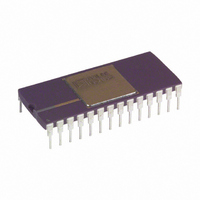
IC,D/A CONVERTER,SINGLE,16-BIT,BICMOS,DIP,28PIN
Manufacturer
Analog Devices Inc
Datasheet
1.AD569JNZ.pdf
(12 pages)
Specifications of AD569BD
Rohs Status
RoHS non-compliant
Settling Time
4µs
Number Of Bits
16
Data Interface
Parallel
Number Of Converters
1
Voltage Supply Source
Dual ±
Operating Temperature
-25°C ~ 85°C
Mounting Type
Through Hole
Package / Case
28-CDIP (0.600", 15.24mm)
Power Dissipation (max)
-
Lead Free Status / RoHS Status
Available stocks
Company
Part Number
Manufacturer
Quantity
Price


AD569
ABSOLUTE MAXIMUM RATINGS*
(T
+V
–V
+V
Digital Inputs
+V
–V
V
V
V
ESD SENSITIVITY
The AD569 features input protection circuitry consisting of large “distributed” diodes and polysilicon
series resistors to dissipate both high-energy discharges (Human Body Model) and fast, low-energy
pulses (Charged Device Model). Per Method 3015.2 of MIL-STD-883C, the AD569 has been
classified as a Category A device.
Proper ESD precautions are strongly recommended to avoid functional damage or performance
degradation. Charges as high as 4000 volts readily accumulate on the human body and test equipment
and discharge without detection. Unused devices must be stored in conductive foam or shunts, and
the foam should be discharged to the destination socket before devices are removed. For further
information on ESD precautions, refer to Analog Devices’ ESD Prevention Manual.
REF
REF
OUT
A
(Pins 4-14, 19-27) to GND (Pin 18) . . . . . . . . . +V
S
REF
S
S
REF
. . . . . . . . . . . . . . . . . . . . . . . .
= +25 C unless otherwise noted)
(Pin 28) to GND (Pin 18) . . . . . . . . . . . . . . –18 V, +0.3 V
(Pin 1) to GND (Pin 18) . . . . . . . . . . . . . . +18 V, –0.3 V
(Pin 1) to –V
Force (Pins 3, 15) to GND (Pin 18) . . . . . . . . . . . . . V
Sense (Pins 2, 16) to GND (Pin 18) . . . . . . . . . . . . . V
(Pin 17) . . . . . . . . . . . . . . . . . . Indefinite Short to GND
Force (Pin 15) to –V
Force (Pin 3) to +V
Model
AD569JN
AD569SD
NOTES
1
2
AD569JP
AD569KN
AD569KP
AD569AD
AD569BD
For details on grade and package offerings screened in accordance with MIL-STD-883, refer to the Analog Devices Military Products Databook
or current AD569/883B data sheet.
D = Ceramic DIP; N = Plastic DIP; P = Plastic Leaded Chip Carrier.
1
S
(Pin 28) . . . . . . . . . . . . . . . +26.4 V, –0.3 V
+25 C
Integral Nonlinearity
REF
0.04%
0.04%
0.024%
0.024%
0.04%
0.024%
0.04%
REF
Sense (Pin 2) . . . . . . . . 16.5 V
Sense (Pin 16) . . . . . . . 16.5 V
Momentary Short to +V
T
0.04%
0.04%
0.024%
0.024%
0.04%
0.024%
0.04%
MIN
–T
MAX
PIN DESIGNATIONS
ORDERING GUIDE
S
Differential Nonlinearity
+25 C
, –0.3 V
1 LSB
1 LSB
1/2 LSB
1/2 LSB
1 LSB
1/2 LSB
1 LSB
S,
–V
S
S
S
–4–
Power Dissipation (Any Package) . . . . . . . . . . . . . . . 1000 mW
Operating Temperature Range
Storage Temperature . . . . . . . . . . . . . . . . . . . –65 C to +150 C
Lead Temperature Range (Soldering, 10 secs) . . . . . . . +300 C
*Stresses above those listed under “Absolute Maximum Ratings” may cause
permanent damage to the device. This is a stress rating only and functional
operation of the device at these or any other conditions above those indicated in the
operational sections of this specification is not implied. Exposure to absolute
maximum rating conditions for extended periods may affect device reliability.
T
Commercial Plastic (JN, KN, JP, KP Versions) 0 C to +70 C
Industrial Ceramic (AD, BD Versions) . . . . –25 C to +85 C
Extended Ceramic (SD Versions) . . . . . . . –55 C to +125 C
1 LSB
1 LSB
1 LSB
1 LSB
1 LSB
1 LSB
1 LSB
MIN
–T
MAX
Temperature
Range
0 C to +70 C
0 C to +70 C
0 C to +70 C
0 C to +70 C
–25 C to +85 C
–25 C to +85 C
–55 C to +125 C
WARNING!
Package
Option
N-28
P-28A
N-28
P-28A
D-28
D-28
D-28
ESD SENSITIVE DEVICE
2
REV. A
Related parts for AD569BD
Image
Part Number
Description
Manufacturer
Datasheet
Request
R

Part Number:
Description:
DPG2 EVAL ADAPTER FOR XILINX BOARDS
Manufacturer:
Analog Devices Inc
Part Number:
Description:
Xilinx FMC Interface
Manufacturer:
Analog Devices Inc
Datasheet:
Part Number:
Description:
Xilinx FMC Interface
Manufacturer:
Analog Devices Inc
Datasheet:
Part Number:
Description:
Xilinx FMC Interface
Manufacturer:
Analog Devices Inc
Datasheet:
Part Number:
Description:
Xilinx FMC Interface
Manufacturer:
Analog Devices Inc
Datasheet:
Part Number:
Description:
Xilinx FMC Interface
Manufacturer:
Analog Devices Inc
Datasheet:
Part Number:
Description:
Xilinx FMC Interface
Manufacturer:
Analog Devices Inc
Datasheet:
Part Number:
Description:
Xilinx FMC Interface
Manufacturer:
Analog Devices Inc
Datasheet:
Part Number:
Description:
AD CONVERTOR, IC, BIT COUNT FOR PROCESSOR
Manufacturer:
Analog Devices Inc

Part Number:
Description:
±1.7g Dual-Axis IMEMS Accelerometer Evaluation Board
Manufacturer:
Analog Devices Inc
Datasheet:
Part Number:
Description:
Inertial Sensor Evaluation System
Manufacturer:
Analog Devices Inc
Datasheet:
Part Number:
Description:
Manufacturer:
Analog Devices Inc
Datasheet: