AD652AQ/+ Analog Devices Inc, AD652AQ/+ Datasheet - Page 5
AD652AQ/+
Manufacturer Part Number
AD652AQ/+
Description
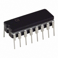
IC,Voltage-to-Frequency Converter,DIP,16PIN
Manufacturer
Analog Devices Inc
Type
Voltage to Frequencyr
Datasheet
1.AD652JPZ.pdf
(28 pages)
Specifications of AD652AQ/+
Rohs Status
RoHS non-compliant
Frequency - Max
2MHz
Full Scale
±50ppm/°C
Linearity
±0.02%
Mounting Type
Through Hole
Package / Case
16-CDIP (0.300", 7.62mm)
Lead Free Status / RoHS Status


ABSOLUTE MAXIMUM RATINGS
Table 2.
Parameter
Total Supply Voltage +V
Maximum Input Voltage (Figure 6)
Maximum Output Current
Amplifier Short-Circuit to Ground
Storage Temperature Range: CERDIP
Storage Temperature Range: PLCC
ESD CAUTION
ESD (electrostatic discharge) sensitive device. Electrostatic charges as high as 4000 V readily accumulate on
the human body and test equipment and can discharge without detection. Although this product features
proprietary ESD protection circuitry, permanent damage may occur on devices subjected to high energy
electrostatic discharges. Therefore, proper ESD precautions are recommended to avoid performance
degradation or loss of functionality.
DEFINITIONS OF SPECIFICATIONS
Gain Error
The gain of a voltage-to-frequency converter is the scale factor
setting that provides the nominal conversion relationship, e.g.,
1 MHz full scale. The gain error is the difference in slope
between the actual and ideal transfer functions for the V-F
converter.
Linearity Error
The linearity error of a V-F is the deviation of the actual
transfer function from a straight line passing through the
endpoints of the transfer function.
Gain Temperature Coefficient
The gain temperature coefficient is the rate of change in full-
scale frequency as a function of the temperature from +25°C to
T
MIN
(Open Collector Output)
or T
MAX
.
S
to −V
S
Ratings
36 V
36 V
50 mA
Indefinite
−65°C to +150°C
−65°C to +150°C
Rev. C | Page 5 of 28
Stresses above those listed under Absolute Maximum Ratings
may cause permanent damage to the device. This is a stress
rating only; functional operation of the device at these or any
other conditions above those indicated in the operational
section of this specification is not implied. Exposure to absolute
maximum rating conditions for extended periods may affect
device reliability.
Table 3. Pin Configurations
Pin No.
1
2
3
4
5
6
7
8
9
10
11
12
13
14
15
16
17
18
19
20
Q-16 Package
+V
TRIM
TRIM
OP AMP OUT
OP AMP “−“
OP AMP “+”
10 VOLT INPUT
−V
C
CLOCK INPUT
FREQ OUT
DIGITAL GND
ANALOG GND
COMP “−“
COMP “+”
COMP REF
OS
S
S
P-20A Package
NC
+V
NC
OP AMP OUT
OP AMP “−“
OP AMP “+”
5 VOLT INPUT
10 VOLT INPUT
8 VOLT INPUT
OPTIONAL 10 V INPUT
−V
C
CLOCK INPUT
FREQ OUT
DIGITAL GND
ANALOG GND
COMP “−“
COMP “+”
NC
COMP REF
OS
S
S
AD652
Related parts for AD652AQ/+
Image
Part Number
Description
Manufacturer
Datasheet
Request
R

Part Number:
Description:
±1.7g Dual-Axis IMEMS Accelerometer Evaluation Board
Manufacturer:
Analog Devices Inc
Datasheet:

Part Number:
Description:
Inertial Sensor Evaluation System
Manufacturer:
Analog Devices Inc
Datasheet:
Part Number:
Description:
Manufacturer:
Analog Devices Inc
Datasheet:
Part Number:
Description:
Manufacturer:
Analog Devices Inc
Datasheet:
Part Number:
Description:
Manufacturer:
Analog Devices Inc
Datasheet:
Part Number:
Description:
Manufacturer:
Analog Devices Inc
Datasheet:
Part Number:
Description:
Manufacturer:
Analog Devices Inc
Datasheet:
Part Number:
Description:
Manufacturer:
Analog Devices Inc
Datasheet:
Part Number:
Description:
Manufacturer:
Analog Devices Inc
Datasheet:
Part Number:
Description:
Manufacturer:
Analog Devices Inc
Datasheet:
Part Number:
Description:
Manufacturer:
Analog Devices Inc
Datasheet:
Part Number:
Description:
Manufacturer:
Analog Devices Inc
Datasheet:
Part Number:
Description:
Manufacturer:
Analog Devices Inc
Datasheet: