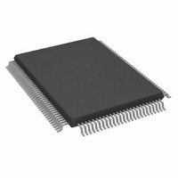
AD6623ASZ Analog Devices Inc, AD6623ASZ Datasheet - Page 29

AD6623ASZ
Manufacturer Part Number
AD6623ASZ
Description
4 Channel, 104 MSPS Digital TSP
Manufacturer
Analog Devices Inc
Datasheet
1.AD6623ABC.pdf
(48 pages)
Specifications of AD6623ASZ
Applications
Transmit Signal Processor
Interface
Serial
Package / Case
128-MQFP, 128-PQFP
Mounting Type
Surface Mount
Lead Free Status / RoHS Status
Lead free / RoHS Compliant
Voltage - Supply
-
Lead Free Status / RoHS Status
Lead free / RoHS Compliant
Available stocks
Company
Part Number
Manufacturer
Quantity
Price
Company:
Part Number:
AD6623ASZ
Manufacturer:
Analog Devices Inc
Quantity:
10 000
Selection of Real and Complex Output Data Types
The AD6623 is capable of outputting both real and complex data.
When in Real mode the QIN input is tied low signaling that all
inputs on the Wideband Input Bus are real and that all outputs
on the Wideband Output Bus are real. The Wideband Input Bus
will be pulled low and no data will be added to the composite
signal if this port is unused (not connected).
If complex data is desired there are two ways this can be obtained.
The first method is to simply set the QIN input of the AD6623
high and to set the Wideband Input Bus low. This allows the AD6623
to output complex data on the Wideband Output Bus. The I data
samples would be identified when QOUT is low and the Q data
samples would be identified when QOUT is high. The second
method of obtaining complex data is to provide a QIN signal that
toggles on every rising edge of the CLK. This could be obtained
by connecting the QOUT of another AD6623 to QIN as shown
in Figure 35. In a cascaded system the QIN of the first AD6623
in the chain would typically be tied high and the QOUT of the
first AD6623 would be connected to the QIN of the following
part. All AD6623s will synchronize themselves to the QIN input
so that the proper samples are always paired and the Wideband
Output bus represents valid complex data samples. Table XVI
shows different parallel input and output data bus formats as a
function of QIN and QOUT.
QIN
Low
High
Pulsed
SYNCHRONIZATION
Three types of synchronization can be achieved with the AD6623.
These are Start, Hop, and Beam. Each is described in detail below.
The synchronization is accomplished with the use of a shadow
register and a Hold-Off counter. See Figure 36 for a simplistic
schematic of the NCO shadow register and NCO Frequency
Hold-Off counter to understand basic operation. Enabling the clock
(AD6623 CLK) for the Hold-Off counter can occur with either
a Soft_Sync (via the Microport), or a Pin Sync. The functions
that include shadow registers to allow synchronization include:
1. Start
2. Hop (NCO Frequency)
3. Beam (NCO Phase Offset)
Hold-Off Counters and Shadow Registers
Hold-Off Counters are used with the five synchronized AD6623
functions:
REV. A
LOGIC1
LOGIC0
• Start of Channel(s)
• RCF Fine Scale output level update
• Power Ramping of Time Slot transmissions
• Frequency Hopping
• Phase Shifting for Beam ControlStart
Figure 35. Cascade Operation of Two AD6623s
Table XVI. Valid Output Bus Data Modes
Q
IN
[17:0]
Wideband Input
IN[17:0]
Real
Zero
Complex
IN
AD6623
Q
OUT
[17:0]
OUT
Q
IN
[17:0]
IN
Output Data Type
OUT[17:0], QOUT
Real
Complex
Complex
AD6623
[16:3]
OUT
14-BIT
DAC
–29–
These are 16-bit counters that are preloaded with a programmable
value upon receipt of a synchronizing pulse. The counter then
counts down to zero and stops. The counters are re-triggerable
during countdown. If the counter is re-triggered, it re-loads its
count value and starts again and may preclude the triggering of
the event as intended. When the count reaches one, a trigger signal
is emitted which causes the desired event (Start, Ramp, Hop, Beam,
Scale) to commence. The counters are clocked with the AD6623
CLK that determines the time resolution of the each count. With
a 104 MHz CLK, the resolution is approximately 10 ns and the
delay range is from approximately 20 ns to 0.6 ms. If a Hold-Off
Counter is loaded with 0, it will not respond to synchronizing
pulses and the event will not be triggered by the hold-off counter.
The AD6623 can “trigger” all of the aforementioned events except
Ramping without a soft-sync, pin-sync, or data-sync. This is
through the use of the Sleep bit for each channel at External
Address 5. Whenever a channel is brought out of sleep mode
(sleep bit = ↓ low) an automatic pulse updates all active and shadow
registers. This feature allows a channel to be reprogrammed while it
is sleeping and then activated with immediate implementation of
the changes.
Shadow Register are provided for three functions, Frequency
Hop, Fine Scale, and Phase Offset. A shadow register precedes
an active register. It holds the next number to be used by the
active register whenever that function’s hold-off counter causes
the active register to be updated with the new value. Active registers
are also updated with the contents of a shadow register any time
the channel is brought out of the sleep mode.
A shadow register is updated during normal programming of the
registers through the Microport. Active registers for frequency,
fine scale and phase offset words can only receive their update
data from a shadow register. When software reads-back a channel’s
programmed values, it is reading back the shadow registers of
the fine scale and phase offset functions but reads the active
frequency register as shown in Figure 36.
Figure 36. NCO Shadow Register and Hold-Off Counter
START
SYNC
SYNC
HOP
NCO SHADOW
32
16
16
REGISTER
HOLDOFF
HOLDOFF
D
HOP
D
START
D
CLR
Q
Q
Q
16
16
CLK
32
REGISTER
COUNTER
HOLDOFF
D
D C = 1
PL
COUNTER
NCO
ENA
D C = 1
PL
START
C = 0
ENA
Q
C = 0
ENA
ACCUMULATOR
NCO PHASE
32
AD6623
RESET PIN
CLR
SET
Q
SLEEP


