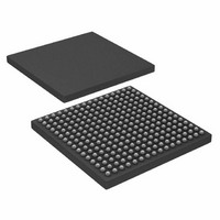
AD6636BBCZ Analog Devices Inc, AD6636BBCZ Datasheet - Page 7

AD6636BBCZ
Manufacturer Part Number
AD6636BBCZ
Description
IC,Downconverter,CMOS,BGA,256PIN,PLASTIC
Manufacturer
Analog Devices Inc
Series
AD6636r
Datasheet
1.AD6636BCPCB.pdf
(80 pages)
Specifications of AD6636BBCZ
Rf Type
Cellular, CDMA2000, EDGE, GPRS, GSM
Number Of Mixers
1
Secondary Attributes
Down Converter
Current - Supply
450mA
Voltage - Supply
3 V ~ 3.6 V
Package / Case
256-CSPBGA
Pin Count
256
Screening Level
Industrial
Package Type
CSPBGA
Lead Free Status / RoHS Status
Lead free / RoHS Compliant
Frequency
-
Gain
-
Noise Figure
-
Lead Free Status / Rohs Status
Compliant
Available stocks
Company
Part Number
Manufacturer
Quantity
Price
Part Number:
AD6636BBCZ
Manufacturer:
ADI/亚德诺
Quantity:
20 000
GENERAL TIMING CHARACTERISTICS
Table 3.
Parameter
CLK TIMING REQUIREMENTS
INPUT WIDEBAND DATA TIMING REQUIREMENTS
PARALLEL OUTPUT PORT TIMING REQUIREMENTS (MASTER)
PARALLEL OUTPUT PORT TIMING REQUIREMENTS (SLAVE)
MISC PINS TIMING REQUIREMENTS
1
2
All timing specifications are valid over the VDDCORE range of 1.7 V to 1.9 V and the VDDIO range of 3.0 V to 3.6 V.
C
LOAD
t
t
t
t
t
t
t
t
t
t
t
t
t
t
t
t
t
t
t
t
t
t
t
t
t
t
t
t
t
t
CLK
CLKL
CLKH
CLKSKEW
SI
HI
SEXP
HEXP
DEXP
DPREQ
DPP
DPIQ
DPCH
DPGAIN
SPA
HPA
PCLK
PCLKL
PCLKH
DPREQ
DPP
DPIQ
DPCH
DPGAIN
SPA
HPA
RESET
DIRP
SSYNC
HSYNC
= 40 pF on all outputs, unless otherwise noted.
CLKx Period (x = A, B, C, D)
CLKx Width Low (x = A, B, C, D)
CLKx Width High (x = A, B, C, D)
CLKA to CLKx Skew (x = B, C, D)
INx [15:0] to ↑CLKx Setup Time (x = A, B, C, D)
INx [15:0] to ↑CLKx Hold Time (x = A, B, C, D)
EXPx [2:0] to ↑CLKx Setup Time (x = A, B, C, D)
EXPx [2:0] to ↑CLKx Hold Time (x = A, B, C, D)
↑CLKx to EXPx[2:0] Delay (x = A, B, C, D)
↑PCLK to ↑Px REQ Delay (x = A, B, C)
↑PCLK to Px [15:0] Delay (x = A, B, C)
↑PCLK to Px IQ Delay (x = A, B, C)
↑PCLK to Px CH[2:0] Delay (x = A, B, C)
↑PCLK to Px Gain Delay (x = A, B, C)
Px ACK to ↑PCLK Setup Time (x = A, B, C)
Px ACK to ↑PCLK Hold Time (x = A, B, C)
PCLK Period
PCLK Low Period
PCLK High Period
↑PCLK to ↑Px REQ Delay (x = A, B, C)
↑PCLK to Px [15:0] Delay (x = A, B, C)
↑PCLK to Px IQ Delay (x = A, B, C)
↑PCLK to Px CH[2:0] Delay (x = A, B, C)
↑PCLK to Px Gain Delay (x = A, B, C)
Px ACK to ↓PCLK Setup Time (x = A, B, C)
Px ACK to ↓PCLK Hold Time (x = A, B, C)
RESET Width Low
CPUCLK/SCLK to IRP Delay
SYNC(0, 1, 2, 3) to ↑CLKA Setup Time
SYNC(0, 1, 2, 3) to ↑CLKA Hold Time
1, 2
Rev. A | Page 7 of 80
Temp
Full
Full
Full
Full
Full
Full
Full
Full
Full
Full
Full
Full
Full
Full
Full
Full
Full
Full
Full
Full
Full
Full
Full
Full
Full
Full
Full
Full
Full
Full
Full
Test Level
I
IV
IV
IV
IV
IV
IV
IV
IV
IV
IV
IV
IV
IV
IV
IV
IV
IV
IV
IV
IV
IV
IV
IV
IV
IV
IV
IV
V
IV
IV
Min
6.66
1.71
1.70
t
0.75
1.13
3.37
1.11
5.98
1.77
2.07
0.48
0.38
0.23
4.59
0.90
5.0
1.7
0.7
4.72
4.8
4.83
4.88
5.08
6.09
1.0
30
0.87
0.67
CLK
− 1.3
Typ
0.5 × t
0.5 × t
0.5 × t
0.5 × t
7.5
CLK
CLK
PCLK
PCLK
10.74
3.86
5.29
5.49
5.35
4.95
8.87
8.48
10.94
10.09
11.49
Max
AD6636
Unit
ns
ns
ns
ns
ns
ns
ns
ns
ns
ns
ns
ns
ns
ns
ns
ns
ns
ns
ns
ns
ns
ns
ns
ns
ns
ns
ns
ns
ns
ns


