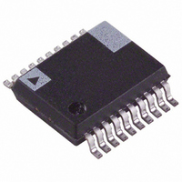
AD7226BRS-REEL Analog Devices Inc, AD7226BRS-REEL Datasheet

AD7226BRS-REEL
Specifications of AD7226BRS-REEL
Related parts for AD7226BRS-REEL
AD7226BRS-REEL Summary of contents
Page 1
FEATURES Four 8-Bit DACs with Output Amplifiers Skinny 20-Lead DIP, SOIC, SSOP, and PLCC Packages Microprocessor-Compatible TTL/CMOS-Compatible No User Trims Extended Temperature Range Operation Single Supply Operation Possible APPLICATIONS Process Control Automatic Test Equipment Automatic Calibration of Large System Parameters, ...
Page 2
AD7226–SPECIFICATIONS DUAL SUPPLY Parameter STATIC PERFORMANCE Resolution Total Unadjusted Error Relative Accuracy Differential Nonlinearity Full-Scale Error Full-Scale Temperature Coefficient Zero Code Error Zero Code Error Temperature Coefficient ± 50 REFERENCE INPUT Voltage Range Input Resistance 3 Input Capacitance DIGITAL INPUTS ...
Page 3
V DD SINGLE SUPPLY All specifications T Parameter STATIC PERFORMANCE Resolution Total Unadjusted Error Differential Nonlinearity REFERENCE INPUT Input Resistance 3 Input Capacitance DIGITAL INPUTS Input High Voltage, V INH Input Low Voltage, V INL Input Leakage ...
Page 4
AD7226 TERMINOLOGY TOTAL UNADJUSTED ERROR This is a comprehensive specification that includes full-scale error, relative accuracy and zero code error. Maximum output voltage is V – 1 LSB (ideal), where 1 LSB (ideal REF 256. The LSB size ...
Page 5
CIRCUIT INFORMATION D/A SECTION The AD7226 contains four identical, 8-bit, voltage mode digital-to- analog converters. The output voltages from the converters have the same polarity as the reference voltage allowing single supply opera- tion. A novel DAC switch pair arrangement ...
Page 6
AD7226 INTERFACE LOGIC INFORMATION Address lines A0 and A1 select which DAC will accept data from the input port. Table I shows the selection table for the four DACs with Figure 4 showing the input control logic. When the WR ...
Page 7
– 2.0 1.5 1.0 0.5 0 –0.5 –1.0 –1.5 –2 112 128 144 160 176 192 208 224 240 ...
Page 8
AD7226 SPECIFICATION RANGES In order for the DACs to operate to their specifications, the reference voltage must be at least 4 V below the V supply voltage. This voltage differential is required for correct generation of bias voltages for the ...
Page 9
V REF MSB DB7 DAC A DB0 LSB DAC B WR DAC DAC D AGND V SS Figure 8. AD7226 Unipolar Output Circuit Table II. Unipolar Code Table DAC Latch Contents MSB LSB Analog Output + V ...
Page 10
AD7226 V REF * AD7226 DAC A AGND 5 V BIAS DIGITAL INPUTS OMITTED FOR CLARITY Figure 10. AGND Bias Circuit For a given V , increasing AGND above system GND will IN reduce the effective V ...
Page 11
STAIRCASE WINDOW COMPARATOR In many test systems important to be able to determine whether some parameter lies within defined limits. The staircase window comparator of Figure 14a is a circuit that can be used, for example, to measure ...
Page 12
AD7226 OFFSET ADJUST Figure 17 shows how the AD7226 can be used to provide pro- grammable input offset voltage adjustment for the AD544 op amp. Each output of the AD7226 can be used to trim the input offset voltage on ...
Page 13
OUTLINE DIMENSIONS 0.210 (5.33) MAX 0.150 (3.81) 0.130 (3.30) 0.115 (2.92) 0.022 (0.56) 0.018 (0.46) 0.014 (0.36) 0.200 (5.08) 0.200 (5.08) 0.125 (3.18) 0.023 (0.58) 0.014 (0.36) 1.060 (26.92) 1.030 (26.16) 0.980 (24.89 0.280 (7.11) 0.250 (6.35) 1 ...
Page 14
AD7226 2.00 MAX 0.05 MIN COPLANARITY 0.10 0.30 (0.0118) 0.10 (0.0039) COPLANARITY 0.10 7.50 7.20 6. 5.60 5.30 8.20 5.00 7.80 7. 1.85 1.75 1.65 0.38 SEATING 0.22 PLANE 0.65 BSC COMPLIANT TO JEDEC STANDARDS MO-150-AE ...
Page 15
... R ORDERING GUIDE 1 Model Temperature Range AD7226BQ −40°C to +85°C AD7226BRSZ −40°C to +85°C AD7226KN −40°C to +85°C AD7226KNZ −40°C to +85°C AD7226KP −40°C to +85°C AD7226KP-REEL −40°C to +85°C AD7226KPZ − ...
Page 16
AD7226 NOTES ©2003-2011 Analog Devices, Inc. All rights reserved. Trademarks and registered trademarks are the property of their respective owners. D00987-0-1/11(D) Rev Page ...


