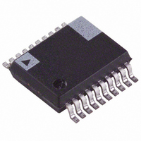
AD7226BRS-REEL Analog Devices Inc, AD7226BRS-REEL Datasheet - Page 9

AD7226BRS-REEL
Manufacturer Part Number
AD7226BRS-REEL
Description
Digital To Analog Converter
Manufacturer
Analog Devices Inc
Datasheet
1.AD7226KRZ.pdf
(16 pages)
Specifications of AD7226BRS-REEL
Rohs Status
RoHS non-compliant
Settling Time
4µs
Number Of Bits
8
Data Interface
Parallel
Number Of Converters
4
Voltage Supply Source
Dual ±
Operating Temperature
-40°C ~ 85°C
Mounting Type
Surface Mount
Package / Case
20-SSOP
Power Dissipation (max)
-
Lead Free Status / RoHS Status
Bipolar Output Operation
Each of the DACs of the AD7226 can be individually config-
ured to provide bipolar output operation. This is possible using
one external amplifier and two resistors per channel. Figure 9
shows a circuit used to implement offset binary coding (bipolar
operation) with DAC A of the AD7226. In this case
REV.
DAC Latch Contents
MSB
1 1 1 1
1 0 0 0
1 0 0 0
0 1 1 1
0 0 0 0
0 0 0 0
V
Note LSB
OUT
D
Figure 8. AD7226 Unipolar Output Circuit
:
=
MSB
WR
LSB
A1
A0
Ê
Á
Ë
1
+
Table II. Unipolar Code Table
=
DB0
DB7
R
R
LSB
1 1 1 1
0 0 0 1
0 0 0 0
1 1 1 1
0 0 0 1
0 0 0 0
(
V
2
1
V
REF
REF
ˆ
˜ ¥
¯
)
(
( )
D V
2
DAC A
DAC B
DAC C
DAC D
–
A REF
8
V
SS
=
V
AGND
)
REF
–
Ê
Á
Ë
Analog Output
0 V
+
+
+
+
+
Ê
Á
Ë
R
R
V
V
V
V
V
256
V
2
1
REF
REF
REF
REF
REF
DD
1
ˆ
˜ ¥
¯
DGND
ˆ
˜
¯
Ê
Á
Ë
Ê
Á
Ë
Ê
Á
Ë
Ê
Á
Ë
Ê
Á
Ë
(
V
255
256
129
256
128
256
127
256
256
1
REF
V
V
V
V
OUT
OUT
OUT
OUT
ˆ
˜
¯
ˆ
˜
¯
ˆ
˜ = +
¯
ˆ
˜
¯
ˆ
˜
¯
)
A
B
C
D
V
REF
2
(2)
(3)
–9–
With R1 = R2
where D
Mismatch between R1 and R2 causes gain and offset errors and
therefore these resistors must match and track over tempera-
ture. Once again the AD7226 can be operated in single supply
or from positive/negative supplies. Table III shows the digital
code versus output voltage relationship for the circuit of Figure 9
with R1 = R2.
AGND BIAS
The AD7226 AGND pin can be biased above system GND
(AD7226 DGND) to provide an offset “zero” analog output
voltage level. Figure 10 shows a circuit configuration to achieve
this for channel A of the AD7226. The output voltage, V
can be expressed as:
where D
(0 £ D £ 255/256).
V
DAC Latch Contents
REF
V
MSB
1 1 1 1
1 0 0 0
1 0 0 0
0 1 1 1
0 0 0 0
0 0 0 0
V
OUT
OUT
A
Table III. Bipolar (Offset Binary) Code Table
A
is a fractional representation of the digital word in latch A.
Figure 9. AD7226 Bipolar Output Circuit
is a fractional representation of the digital input word
A V
=
=
(
2
DAC A
D
V
BIAS
REF
A
AD7226
V
LSB
1 1 1 1
0 0 0 1
0 0 0 0
1 1 1 1
0 0 0 1
0 0 0 0
–
SS
+
1
)
D V
¥
AGND
A
V
*
( )
REF
IN
V
DGND
DD
Analog Output
0 V
+
+
–V
–V
–
V
V
V
V
REF
REF
REF
REF
REF
OUT
* DIGITAL INPUTS OMITTED
R1, R2 = 10k
FOR CLARITY
R1
A
Ê
Á
Ë
Ê
Á
Ë
Ê
Á
Ë
Ê
Á
Ë
Ê
Á
Ë
127
128
128
128
127
128
128
128
1
1
AD7226
–15V
+15V
ˆ
˜
¯
ˆ
˜
¯
ˆ
˜
¯
ˆ
˜
¯
ˆ
˜ =
¯
R2
–
V
0.1%
REF
OUT
V
OUT
A,
(4)
(5)


