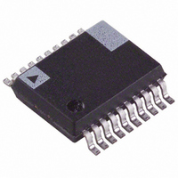
AD73311ARSZ Analog Devices Inc, AD73311ARSZ Datasheet - Page 29

AD73311ARSZ
Manufacturer Part Number
AD73311ARSZ
Description
IC,PCM CODEC,SINGLE,CMOS,SSOP,20PIN,PLASTIC
Manufacturer
Analog Devices Inc
Datasheet
1.AD73311ARZ.pdf
(36 pages)
Specifications of AD73311ARSZ
Number Of Bits
16
Number Of Channels
2
Power (watts)
50mW
Voltage - Supply, Analog
3V
Voltage - Supply, Digital
3V
Package / Case
20-SSOP
Lead Free Status / RoHS Status
Lead free / RoHS Compliant
Available stocks
Company
Part Number
Manufacturer
Quantity
Price
Part Number:
AD73311ARSZ
Manufacturer:
ADI/亚德诺
Quantity:
20 000
Part Number:
AD73311ARSZ-REEL7
Manufacturer:
ADI/亚德诺
Quantity:
20 000
APPENDIX B
Programming a Single AD73311 for Mixed Mode Operation
This section describes a typical sequence in programming a
single codec to operate in mixed mode. The device is connected
in Nonframe Sync Loop-Back Mode (see Figure 14), which
allows the DSP’s Tx Reg to determine how many words are sent
to the device. In Step 1, the part has just been reset and on the
first output event the codec presents an invalid output word
The DSP’s Tx Reg contains a control word that programs CRA
with the data word 0x03, which will put the device in mixed
mode. In Step 2, the control word from the DSP’s Tx Reg has
been sent to the codec’s SPORT and the output word has been
received by the DSP’s Rx Reg. The Tx Register raises the
SDIFS to send a control word that will program CRB of the
codec. In Step 3 the SCLK and sample rate are set by program-
ming CRB. In Step 4, the analog sections of the device are
*ADC SAMPLES DURING PROGRAM MODE ARE INVALID.
STEP 1
STEP 2
STEP 3
STEP 4
STEP 5
STEP 6
STEP 7
STEP 8
1 0 000 000 00000011
1 0 000 001 00001111
1 0 000 010 00000001
1 0 000 000 00000001
0100 0000 0000 0000
0011 1111 1111 1111
0011 1111 1111 1111
0100 0000 0000 0000
CONTROL WORD 1
CONTROL WORD 1
CONTROL WORD 1
CONTROL WORD 1
DAC WORD 1
DAC WORD 1
DAC WORD 1
DSP TX REG
DSP TX REG
DSP TX REG
DSP TX REG
DSP TX REG
DSP TX REG
DAC WORD 1
DSP TX REG
DSP TX REG
1 0 000 011 00100000
1 0 000 001 00001111
1 0 000 010 00000001
1 0 000 000 00000011
0000 0000 0000 0000
0100 0000 0000 0000
0100 0000 0000 0000
0011 1111 1111 1111
CONTROL WORD 1
CONTROL WORD 1
CONTROL WORD 1
CONTROL WORD 1
1
.
ADC WORD 1 *
ADC WORD 1
DAC WORD 1
DAC WORD 1
DEVICE 1
DEVICE 1
DEVICE 1
DEVICE 1
DEVICE 1
DEVICE 1
DEVICE 1
DEVICE 1
powered up by programming CRC, while in Step 5, the encoder
gain is set to 0 dB via CRD. In Step 6, the DAC register is
updated by the contents of the serial register. Alternately, a
register read cycle could be introduced instead of the DAC load
in Step 6
cycle.
NOTES
1
2
Data output by the codec in program mode is invalid and should not be inter-
In mixed mode, it may be necessary to terminate a control word write to a
preted as ADC data. The only exception to this is output caused by register
reads or CEE being enabled on control word writes.
device with a control word read to that device in order to ensure that the next
ADC sample is correct. Alternatively the ADC word can either be discarded or,
if this is not possible, it can be rebuilt by incrementing the “address field”
within the 16-bit word.
2
. Steps 7 and 8 show another ADC read, DAC write
XXXX XXXX XXXX XXXX
XXXX XXXX XXXX XXXX
XXXX XXXX XXXX XXXX
XXXX XXXX XXXX XXXX
XXXX XXXX XXXX XXXX
XXXX XXXX XXXX XXXX
1000 0000 0000 0000
0000 0000 0000 0000
ADC WORD 1 *
DSP RX REG
DON'T CARE
ADC WORD 1
DSP RX REG
DSP RX REG
DSP RX REG
DSP RX REG
DSP RX REG
DON'T CARE
DSP RX REG
DON'T CARE
DON'T CARE
DON'T CARE
DON'T CARE
DSP RX REG
AD73311


