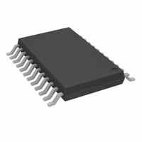
AD7492ARUZ-REEL7 Analog Devices Inc, AD7492ARUZ-REEL7 Datasheet

AD7492ARUZ-REEL7
Manufacturer Part Number
AD7492ARUZ-REEL7
Description
IC,A/D CONVERTER,SINGLE,12-BIT,TSSOP,24PIN
Manufacturer
Analog Devices Inc
Datasheet
1.AD7492ARUZ.pdf
(16 pages)
Specifications of AD7492ARUZ-REEL7
Number Of Bits
12
Sampling Rate (per Second)
1M
Data Interface
Parallel
Number Of Converters
1
Power Dissipation (max)
16.5mW
Voltage Supply Source
Analog and Digital
Operating Temperature
-40°C ~ 85°C
Mounting Type
Surface Mount
Package / Case
24-TSSOP (0.173", 4.40mm Width)
Lead Free Status / RoHS Status
Lead free / RoHS Compliant
For Use With
EVAL-AD7492CBZ - BOARD EVALUATION FOR AD7492
Lead Free Status / RoHS Status
Lead free / RoHS Compliant
Available stocks
Company
Part Number
Manufacturer
Quantity
Price
Part Number:
AD7492ARUZ-REEL7
Manufacturer:
ADI/亚德诺
Quantity:
20 000
a
GENERAL DESCRIPTION
The AD7492 and AD7492-5 are 12-bit high-speed, low power,
successive-approximation ADCs. The parts operate from a
single 2.7 V to 5.25 V power supply and feature throughput rates
up to 1.25 MSPS. They contain a low-noise, wide bandwidth
track/hold amplifier that can handle bandwidths up to 10 MHz.
The conversion process and data acquisition are controlled using
standard control inputs allowing easy interface to microproces-
sors or DSPs. The input signal is sampled on the falling edge of
CONVST and conversion is also initiated at this point. The
BUSY goes high at the start of conversion and goes low 880 ns
(AD7492) or 680 ns (AD7492-5) later to indicate that the con-
version is complete. There are no pipeline delays associated with
the part. The conversion result is accessed via standard CS and
RD signals over a high-speed parallel interface.
The AD7492 uses advanced design techniques to achieve very
low power dissipation at high throughput rates. With 5 V
supplies and 1.25 MSPS, the average current consumption
AD7492-5 is typically 2.75 mA. The part also offers flexible
power/throughput rate management.
It is also possible to operate the part in a full sleep mode and a
partial sleep mode, where the part wakes up to do a conversion
and automatically enters a sleep mode at the end of conversion.
The type of sleep mode is hardware selected by the PS/FS pin.
Using these sleep modes allows very low power dissipation num-
bers at lower throughput rates.
The analog input range for the part is 0 to REF IN. The 2.5 V
reference is supplied internally and is available for external refer-
encing. The conversion rate is determined by the internal clock.
1.25 MSPS, 16 mW Internal REF and CLK,
PRODUCT HIGHLIGHTS
1. High Throughput with Low Power Consumption
2. Flexible Power/Throughput Rate Management
3. No Pipeline Delay
4. Flexible Digital Interface
5. Fewer Peripheral Components
CONVST
The AD7492-5 offers 1.25 MSPS throughput with 16 mW
power consumption.
The conversion time is determined by an internal clock. The
part also features two sleep modes, partial and full, to maxi-
mize power efficiency at lower throughput rates.
The part features a standard successive-approximation ADC
with accurate control of the sampling instant via a CONVST
input and once-off conversion control.
The V
digital pins.
The AD7492 optimizes PCB space by using an internal
Reference and internal CLK.
VIN
DRIVE
2.5V
REF
FUNCTIONAL BLOCK DIAGRAM
AD7492
AVDD
feature controls the voltage levels on the I/O
T/H
DVDD
BUF
12-Bit Parallel ADC
AGND
12-BIT SAR
CONTROL
REF OUT
LOGIC
ADC
OSCILLATOR
CLOCK
DGND
DRIVERS
OUTPUT
VDRIVE
AD7492
DB11
DB0
PS/FS
CS
RD
BUSY


