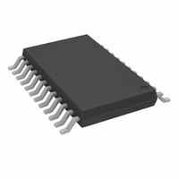
AD7492ARUZ-REEL7 Analog Devices Inc, AD7492ARUZ-REEL7 Datasheet - Page 11

AD7492ARUZ-REEL7
Manufacturer Part Number
AD7492ARUZ-REEL7
Description
IC,A/D CONVERTER,SINGLE,12-BIT,TSSOP,24PIN
Manufacturer
Analog Devices Inc
Datasheet
1.AD7492ARUZ.pdf
(16 pages)
Specifications of AD7492ARUZ-REEL7
Number Of Bits
12
Sampling Rate (per Second)
1M
Data Interface
Parallel
Number Of Converters
1
Power Dissipation (max)
16.5mW
Voltage Supply Source
Analog and Digital
Operating Temperature
-40°C ~ 85°C
Mounting Type
Surface Mount
Package / Case
24-TSSOP (0.173", 4.40mm Width)
Lead Free Status / RoHS Status
Lead free / RoHS Compliant
For Use With
EVAL-AD7492CBZ - BOARD EVALUATION FOR AD7492
Lead Free Status / RoHS Status
Lead free / RoHS Compliant
Available stocks
Company
Part Number
Manufacturer
Quantity
Price
Part Number:
AD7492ARUZ-REEL7
Manufacturer:
ADI/亚德诺
Quantity:
20 000
this mode a new conversion should not be initiated until 140 ns
after BUSY goes low. This acquisition time allows the track/hold
circuit to accurately acquire the input signal. As mentioned
earlier, a read should not be done during a conversion. This
mode facilitates the fastest throughput times for the AD7492.
M
Figure 11 shows AD7492 in Mode 2 operation where the ADC
goes into either partial or full sleep mode after conversion. The
CONVST line is brought low to initiate a conversion and remains
low until after the end of conversion. If CONVST goes high and
low again while BUSY is high, the conversion is restarted. Once
the BUSY line goes from a high to a low, the CONVST line has its
status checked and, if low, the part enters a sleep mode. The
type of sleep mode the AD7492 enters depends on what ever
way the PS/FS pin is hardwired. If the PS/FS pin is tied high,
the AD7492 will enter partial sleep mode. If the PS/FS pin is
tied low, the AD7492 will enter full sleep mode.
The device wakes up again on the rising edge of the CONVST
signal. From partial sleep the AD7492 is capable of starting
ode 2 (Partial or Full Sleep Mode)
CONVST
BUSY
DBx
RD
CS
CONVST
CONVST
BUSY
BUSY
DBx
DBx
CS
RD
t
CONVERT
t
t
2
2
DATA N
t
t
CONVERT
CONVERT
t
4
t
3
conversions typically 1 µs after the rising edge of CONVST. The
CONVST line can go from a high to a low during the wake-up
time, but the conversion will still not be initiated until after 1 µs.
We recommend that conversion should not be initiated until at
least 20 µs of the wake-up time has elapsed. This will ensure that
the AD7492 has stabilized to within 0.5 LSB of the analog input
value. After 1 µs, the AD7492 will have only stabilized to within
approximately 3 LSB of the input value. From full sleep this wake-
up time is typically 500 µs. In all cases the BUSY line will only go
high once CONVST goes low. Superior power performance can
be achieved in these modes of operation by waking up the
AD7492 only to carry out a conversion. The optimum power
performance is obtained when using full sleep mode as the ADC
comparator, Reference buffer and Reference circuit is powered
down. While in partial sleep mode, only the ADC comparator is
powered down and the reference buffer is put into a low power
mode. The 100 nF capacitor on the REF OUT pin is kept charged
up by the reference buffer in partial sleep mode while in full
sleep mode this capacitor slowly discharges. This explains why
the wake-up time is shorter in partial sleep mode. In both sleep
modes the clock oscillator circuit is powered down.
t
6
t
5
DATA N+1
t
CS
t
9
t
9
7
t
t
10
8
t
WAKEUP
RD
AD7492


