AD7524TQ Analog Devices Inc, AD7524TQ Datasheet - Page 3
AD7524TQ
Manufacturer Part Number
AD7524TQ
Description
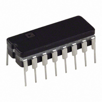
IC,D/A CONVERTER,SINGLE,8-BIT,CMOS,DIP,16PIN
Manufacturer
Analog Devices Inc
Datasheet
1.AD7524JNZ.pdf
(8 pages)
Specifications of AD7524TQ
Rohs Status
RoHS non-compliant
Settling Time
250ns
Number Of Bits
8
Data Interface
Parallel
Number Of Converters
1
Voltage Supply Source
Single Supply
Power Dissipation (max)
30mW
Operating Temperature
-40°C ~ 85°C
Mounting Type
Through Hole
Package / Case
16-CDIP (0.300", 7.62mm)
Lead Free Status / RoHS Status
Available stocks
Company
Part Number
Manufacturer
Quantity
Price

Company:
Part Number:
AD7524TQ/883B 5962-8770002EA
Manufacturer:
MP
Quantity:
7


REV. B
*Stresses above those listed under “Absolute Maximum Ratings” may cause
TERMINOLOGY
RELATIVE ACCURACY: A measure of the deviation from a
straight line through the end points of the DAC transfer function.
Normally expressed as a percentage of full scale range. For the
AD7524 DAC, this holds true over the entire V
RESOLUTION: Value of the LSB. For example, a unipolar con-
verter with n bits has a resolution of (2
verter of n bits has a resolution of [2
way implies linearity.
GAIN ERROR: Gain Error is a measure of the output error be-
tween an ideal DAC and the actual device output. It is measured
ABSOLUTE MAXIMUM RATINGS*
(T
V
V
V
Digital Input Voltage to GND . . . . . . . . –0.3 V to V
OUT1, OUT2 to GND . . . . . . . . . . . . . –0.3 V to V
CAUTION
ESD (electrostatic discharge) sensitive device. Electrostatic charges as high as 4000 V readily
accumulate on the human body and test equipment and can discharge without detection.
Although the AD7524 features proprietary ESD protection circuitry, permanent damage may
occur on devices subjected to high energy electrostatic discharges. Therefore, proper ESD
precautions are recommended to avoid performance degradation or loss of functionality.
permanent damage to the device. This is a stress rating only and functional
operation of the device at these or any other conditions above those indicated in the
operational sections of this specification is not implied. Exposure to absolute
maximum rating conditions for extended periods may affect device reliability.
DD
RFB
REF
A
= +25 C, unless otherwise noted)
to GND . . . . . . . . . . . . . . . . . . . . . . . . . . . –0.3 V, +17 V
to GND . . . . . . . . . . . . . . . . . . . . . . . . . . . . . . . . . 25 V
to GND . . . . . . . . . . . . . . . . . . . . . . . . . . . . . . . . . 25 V
DIP, SOIC
–(n–1)
–n
) (V
] [V
REF
REF
REF
). A bipolar con-
]. Resolution in no
range.
PIN CONFIGURATIONS
DD
DD
+0.3 V
+0.3 V
PLCC
–3–
Power Dissipation (Any Package)
Operating Temperature
Storage Temperature . . . . . . . . . . . . . . . . . . –65 C to +150 C
Lead Temperature (Soldering, 10 secs) . . . . . . . . . . . +300 C
with all 1s in the DAC after offset error has been adjusted out
and is expressed in LSBs. Gain Error is adjustable to zero with
an external potentiometer.
FEEDTHROUGH ERROR: Error caused by capacitive cou-
pling from V
OUTPUT CAPACITANCE: Capacity from OUT1 and
OUT2 terminals to ground.
OUTPUT LEAKAGE CURRENT: Current which appears
on OUT1 terminal with all digital inputs LOW or on OUT2
terminal when all inputs are HIGH. This is an error current
which contributes an offset voltage at the amplifier output.
To +75 C . . . . . . . . . . . . . . . . . . . . . . . . . . . . . . . . 450 mW
Commercial (J, K, L) . . . . . . . . . . . . . . . . . –40 C to +85 C
Industrial (A, B, C) . . . . . . . . . . . . . . . . . . –40 C to +85 C
Extended (S, T, U) . . . . . . . . . . . . . . . . . –55 C to +125 C
Derates above 75 C by . . . . . . . . . . . . . . . . . . . . 6 mW/ C
REF
to output with all switches OFF.
WARNING!
LCCC
ESD SENSITIVE DEVICE
AD7524
Related parts for AD7524TQ
Image
Part Number
Description
Manufacturer
Datasheet
Request
R

Part Number:
Description:
±1.7g Dual-Axis IMEMS Accelerometer Evaluation Board
Manufacturer:
Analog Devices Inc
Datasheet:

Part Number:
Description:
Inertial Sensor Evaluation System
Manufacturer:
Analog Devices Inc
Datasheet:
Part Number:
Description:
Manufacturer:
Analog Devices Inc
Datasheet:
Part Number:
Description:
Manufacturer:
Analog Devices Inc
Datasheet:
Part Number:
Description:
Manufacturer:
Analog Devices Inc
Datasheet:
Part Number:
Description:
Manufacturer:
Analog Devices Inc
Datasheet:
Part Number:
Description:
Manufacturer:
Analog Devices Inc
Datasheet:
Part Number:
Description:
Manufacturer:
Analog Devices Inc
Datasheet:
Part Number:
Description:
Manufacturer:
Analog Devices Inc
Datasheet:
Part Number:
Description:
Manufacturer:
Analog Devices Inc
Datasheet:
Part Number:
Description:
Manufacturer:
Analog Devices Inc
Datasheet:
Part Number:
Description:
Manufacturer:
Analog Devices Inc
Datasheet:
Part Number:
Description:
Manufacturer:
Analog Devices Inc
Datasheet: