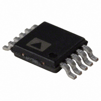
AD7789BRM Analog Devices Inc, AD7789BRM Datasheet - Page 13

AD7789BRM
Manufacturer Part Number
AD7789BRM
Description
Low Power 24-Bit SD ADC I.C.
Manufacturer
Analog Devices Inc
Datasheet
1.AD7789BRMZ.pdf
(20 pages)
Specifications of AD7789BRM
Rohs Status
RoHS non-compliant
Number Of Bits
24
Sampling Rate (per Second)
16.6
Data Interface
DSP, MICROWIRE™, QSPI™, Serial, SPI™
Number Of Converters
1
Power Dissipation (max)
230µW
Voltage Supply Source
Single Supply
Operating Temperature
-40°C ~ 105°C
Mounting Type
Surface Mount
Package / Case
10-TFSOP (0.118", 3.00mm Width)
Lead Free Status / RoHS Status
Contains lead / RoHS non-compliant
Available stocks
Company
Part Number
Manufacturer
Quantity
Price
Part Number:
AD7789BRMZ
Manufacturer:
ADI/亚德诺
Quantity:
20 000
MODE REGISTER
(RS1, RS0 = 0, 1; Power-On/Reset = 0x02)
The mode register is an 8-bit register from which data can be read from or written to. This register is used to configure the ADC for
range, to set unipolar or bipolar mode, to enable or disable the buffer, or to place the device into power-down mode. Table 11 outlines the
bit designations for the mode register. MR0 through MR7 indicate the bit locations, MR denoting the bits are in the mode register. MR7
denotes the first bit of the data stream. The number in brackets indicates the power-on/reset default status of that bit. Any write to the
setup register resets the modulator and filter, and sets the RDY bit.
MSB
MR7
MD1[0]
Table 11. Mode Register Bit Designations
Bit Location
MR7 to MR6
MR5 to MR3
MR2
MR1
MR0
Table 12. Operating Modes
MD1
0
0
1
1
DATA REGISTER
(RS1, RS0 = 1, 1; Power-On/Reset = 0x0000 for the AD7788 and 0x000000 for the AD7789)
The conversion result from the ADC is stored in this data register. This is a read only register. On completion of a read operation from
this register, the RDY bit/pin is set.
Bit Name
MD1 to MD0
0
U/B
1
0
MR6
MD0[0]
MD0
0
1
0
1
These bits must be programmed with a Logic 0 for correct operation.
This bit must be programmed with a Logic 1 for correct operation.
This bit must be programmed with a Logic 0 for correct operation.
Description
Mode Select Bits. These bits select between continuous conversion mode, single conversion mode, and
standby mode. In continuous conversion mode, the ADC continuously performs conversions and places
the result in the data register. DOUT/ RDY goes low when a conversion is complete. The user can read these
conversions by placing the device in continuous read mode whereby the conversions are automatically
placed on the DOUT/ RDY line when SCLK pulses are applied. Alternatively, the user can instruct the ADC to
output the conversion by writing to the communications register. After power-on, the first conversion is
available after a period 2/ f
conversion mode, the ADC is placed in power-down mode when conversions are not being performed.
When single conversion mode is selected, the ADC powers up (which takes 1 ms) and performs a single
conversion, requiring a duration of 2/f
goes low, and the ADC returns to power-down mode. The conversion remains in the data register and
DOUT/ RDY remains active (low) until the data is read or another conversion is performed (see Table 12).
Unipolar/Bipolar Bit. Set by user to enable unipolar coding; that is, zero differential input results in
000…000 output, and a full-scale differential input results in 111…111 output. Cleared by the user to
enable bipolar coding. Negative full-scale differential input results in an output code of 000…000, zero
differential input results in an output code of 100…000, and a positive full-scale differential input results in
an output code of 111…111.
MR5
0[0]
Mode
Continuous conversion mode (default)
Reserved
Single conversion mode
Power-down mode
MR4
0[0]
ADC
Rev. B | Page 13 of 20
while subsequent conversions are available at a frequency of f
ADC
MR3
0[0]
. The conversion result is placed in the data register, DOUT/ RDY
MR2
U/B[0]
MR1
1[1]
AD7788/AD7789
ADC
MR0
0[0]
. In single
LSB


