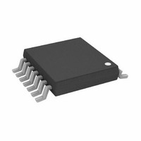
AD8304ARU Analog Devices Inc, AD8304ARU Datasheet - Page 17

AD8304ARU
Manufacturer Part Number
AD8304ARU
Description
Logarithmic Amplifier IC
Manufacturer
Analog Devices Inc
Type
Logarithmic Converterr
Datasheet
1.AD8304ARUZ-RL7.pdf
(20 pages)
Specifications of AD8304ARU
No. Of Amplifiers
1
No. Of Pins
14
Operating Temperature Range
-40°C To +85°C
Slew Rate
15V/µs
Peak Reflow Compatible (260 C)
No
Input Bias Current
400nA
Supply Voltage
5.5V
Bandwidth
10MHz
Rohs Status
RoHS non-compliant
Design Resources
Interfacing ADL5315 to Translinear Logarithmic Amplifier (CN0056) Interfacing ADL5317 High Side Current Mirror to a Translinear Logarithmic Amplifier in an Avalanche Photodiode Power Detector
Applications
Fiber Optics
Mounting Type
Surface Mount
Package / Case
14-TSSOP
Lead Free Status / RoHS Status
Contains lead / RoHS non-compliant
Available stocks
Company
Part Number
Manufacturer
Quantity
Price
Part Number:
AD8304ARU
Manufacturer:
ADI/亚德诺
Quantity:
20 000
Part Number:
AD8304ARU-REEL
Manufacturer:
ADI/亚德诺
Quantity:
20 000
Company:
Part Number:
AD8304ARU-REEL7
Manufacturer:
AD
Quantity:
2 356
Part Number:
AD8304ARUZ
Manufacturer:
AD
Quantity:
20 000
Part Number:
AD8304ARUZ-REEL7
Manufacturer:
ADI/亚德诺
Quantity:
20 000
Company:
Part Number:
AD8304ARUZ-RL7
Manufacturer:
AME
Quantity:
14 500
Programmable Multidecade Current Source
The AD8304 supports a wide variety of general (nonoptical)
applications. For example, the need frequently arises in test
equipment to provide an accurate current that can be varied over
many decades. This can be achieved using a logarithmic amplifier
as the measuring device in an inverse function loop, as illustrated
in Figure 16. This circuit generates the current:
The principle is as follows. The current in QA is forced to supply
a certain I
V
the internal op amp and capacitor C1, with a time constant formed
with the internal 5 kΩ resistor. The choice of C1 in this example
ensures loop stability over the full eight-decade range of output
currents; C2 reduces phase lag. The system is completed with a
10-bit MDAC using V
to 1.6 V FS by R1 and R2 (whose parallel sum is also 5 kΩ).
Transistor QA may be a single bipolar device, which will result in
a small alpha error in I
branch), or a Darlington pair or an MOS device, either of which
ensure a negligible difference between I
the bipolar pair is used. The output voltage compliance is deter-
mined by the collector breakdown voltage of these transistors,
while the minimum voltage depends on where VSUM is placed.
Optional components could be added to put this node and VNEG
at a low enough bias to allow the voltage to go slightly below ground.
Many variations of this basic circuit are possible. For example, the
current can be continuously controlled by a simple voltage, or
by a second current. Larger output currents can be controlled by
setting V
Characterization Setups and Methods
During the primary characterization of the AD8304, the device
was treated as a high precision current-in logarithmic amplifier
(converter). Rather than attempting to accurately generate photo-
currents by illuminating a photodiode, precision current sources,
like the Keithley 236, were used as input sources. Great care was
taken when applying the low level input currents. The triax output
of the current source was used with the guard connected to VSUM
at the characterization board. On the board the input trace was
guarded by connecting adjacent traces and a portion of an internal
copper layer to the VSUM Pins. One obvious reason for the care
was leakage current. With 0.5 V as the nominal bias on the
INPT Pin, a resistance of 50 GΩ to ground would cause 10 pA
of leakage, or about one decibel of error at the low end of the
measurement range. Additionally, the high output resistance of
the current source and the long signal cable lengths commonly
needed in characterization make a good receiver for 60 Hz emis-
sions. Good guarding techniques help to reduce the pickup of
unwanted signals.
REV. A
LOG
I
, and nulling this error by integration. This is performed by
SRC
SUM
PD
=
100
by measuring the error between a setpoint V
to zero and using a current shunt divider.
pA
×
10
REF
SRC
(
V
as its reference, whose output is scaled
(the current is monitored in the emitter
SPT
/ .
0 2
)
PD
and I
SRC
. In this example,
SPT
and
(17)
–17–
The primary characterization setup shown in Figure 18 is used to
measure the static performance, logarithmic conformance, slope
and intercept, buffer offset and V
the performance of the VPDB Pin functions. For the dynamic tests,
such as noise and bandwidth, more specialized setups are used.
Figure 19 shows the configuration used to measure the buffer
amplifier bandwidth. The AD8138 Evaluation Board provides a
dc offset at the buffer input, allowing measurement in single-supply
mode. The network analyzer input impedance was set to 1 MΩ.
+IN
EVALUATION
KEITHLEY 236
AD8138
BOARD
*SIGNAL: INPT;
Figure 19. Configuration for Buffer Amplifier
Bandwidth Measurement
GUARD: VSUM;
SHIELD: GROUND
Figure 18. Primary Characterization Setup
CONNECTOR*
A
B
OUTPUT INPUT INPUTA
TRIAX
SPLITTER
POWER
ANALYZER
NETWORK
HP 3577A
INPT
PWDN VNEG
VSUM
CHARACTERIZATION
DC MATRIX, DC SUPPLIES, DMM
INPUTB
REF
AD8304
VPDB
1
2
3
4
5
6
7
BOARD
VNEG
PWDN
VSUM
INPT
VSUM
VPDB
VREF
drift with temperature, and
AD8304
VPOS
VREF
ACOM
BFNG
VLOG
VOUT
VPS1
VPS2
BFIN
VLOG
VOUT
AD8304
BFIN
14
13
12
11
10
9
8
49.9
RIBBON
CABLE
0.1 F
+V
S


