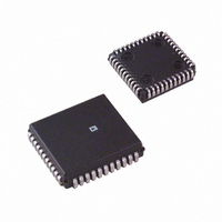
AD8600APZ Analog Devices Inc, AD8600APZ Datasheet - Page 6

AD8600APZ
Manufacturer Part Number
AD8600APZ
Description
16 CHANNEL 8-BIT MULT.DAC
Manufacturer
Analog Devices Inc
Datasheet
1.AD8600APZ-REEL.pdf
(16 pages)
Specifications of AD8600APZ
Rohs Compliant
YES
Settling Time
1µs
Number Of Bits
8
Data Interface
Parallel
Number Of Converters
16
Voltage Supply Source
Analog and Digital, Dual ±
Power Dissipation (max)
175mW
Operating Temperature
-40°C ~ 85°C
Mounting Type
Surface Mount
Package / Case
44-PLCC
Lead Free Status / RoHS Status
Lead free / RoHS Compliant
Available stocks
Company
Part Number
Manufacturer
Quantity
Price
Company:
Part Number:
AD8600APZ
Manufacturer:
Analog Devices Inc
Quantity:
10 000
Part Number:
AD8600APZ
Manufacturer:
ADI/亚德诺
Quantity:
20 000
Company:
Part Number:
AD8600APZ-REEL
Manufacturer:
Analog Devices Inc
Quantity:
10 000
AD8600
TRANSFER EQUATIONS
Output Voltage
where i is the DAC channel number and D is the decimal value
of the DAC register data.
EN R/W CS LD
–
L
+
L
L
L
+
L
X
X
X
X
X
L
NOTES
1
2
+ symbol means positive edge of control input line.
– symbol means negative edge of control input line.
X
X
X
X
L
L
L
L
H
H
X
X
X
X
H
H
H
H
L
L
L
+
L
+
H
X
H
L
L
–
L
+
L
H
H
H
H
H
X
X
H
H
Table I. Truth Table
RS
H
H
H
H
H
H
H
H
H
H
X
L
+
+
O
i
= D
Operation
Write to DAC Register
Update DAC Register
Update DAC Register
Latches DAC Register
Latches DAC Register
DAC Register Transparent
Write to Input Register
Load Data to Input Register at
Decoded Address
Latches Data in Input Register at
Decoded Address
Latches Data in Input Register at
Decoded Address
Readback Input Registers
Input Register Readback (Data
Access)
Hi-Z Readback Disconnects from
Bus
Hi-Z on Data Bus
Reset
Clear All Registers to Zero,
V
Latches All Registers to Zero
CS = Low; Input Register Ready
for R/W, DAC Register Latched
to Zero
OUT
V
256
REF
= 0 V
–6–
Decoded DAC Register
where A is the decimal value of the decoded address bits A3,
A2, A1, A0 (LSB).
Address, CS, R/W and data inputs should be stable prior to acti-
vation of the active low EN input. Input registers are transpar-
ent when EN is low. When EN returns high, data is latched into
the decoded input register. When the load strobe LD and EN
pins are active low, all input register data is transferred to the
DAC registers. The DAC registers are transparent while they
are enabled.
A3
(MSB)
0
0
0
0
0
0
0
0
1
1
1
1
1
1
1
1
A2
0
0
0
0
1
1
1
1
0
0
0
0
1
1
1
1
(Binary)
Table II. Address Decode Table
0
0
1
1
0
0
1
1
0
0
1
1
0
0
1
A1
1
O
(LSB)
A0
0
1
0
1
0
1
0
1
0
1
0
1
0
1
0
1
i
= A
Addr
Code
(Hex)
0
1
2
3
4
5
6
7
8
9
A
B
C
D
E
F
DAC
Updated
O0
O1
O2
O3
O4
O5
O6
O7
O8
O9
O10
O11
O12
O13
O14
O15
REV. 0


