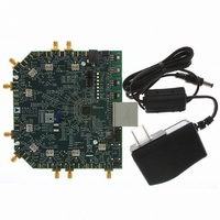
AD9222-65EBZ Analog Devices Inc, AD9222-65EBZ Datasheet - Page 37

AD9222-65EBZ
Manufacturer Part Number
AD9222-65EBZ
Description
Octal 12 Bit, 65 MSPS Serial LVDS ADC EB
Manufacturer
Analog Devices Inc
Datasheet
1.AD9222ABCPZRL7-50.pdf
(60 pages)
Specifications of AD9222-65EBZ
Number Of Adc's
8
Number Of Bits
12
Sampling Rate (per Second)
65M
Data Interface
Serial
Inputs Per Adc
2 Single
Input Range
2 Vpp
Power (typ) @ Conditions
910mW @ 65MSPS
Voltage Supply Source
Single Supply
Operating Temperature
-40°C ~ 85°C
Utilized Ic / Part
AD9222
Kit Application Type
Data Converter
Application Sub Type
ADC
Features
Serial LVDS, Data And Frame Clock Outputs, 325MHz Full-power Analog Bandwidth
Lead Free Status / RoHS Status
Lead free / RoHS Compliant
Lead Free Status / RoHS Status
Lead free / RoHS Compliant
Table 16. Memory Map Register
Addr.
(Hex)
Chip Configuration Registers
00
01
02
Device Index and Transfer Registers
04
05
FF
ADC Functions
08
09
0D
Parameter Name
chip_port_config
chip_id
chip_grade
device_index_2
device_index_1
device_update
modes
clock
test_io
(MSB)
Bit 7
0
X
X
X
X
X
X
User test mode
00 = off (default)
01 = on, single alternate
10 = on, single once
11 = on, alternate once
Bit 6
LSB first
1 = on
0 = off
(default)
Child ID [6:4]
(identify device variants of Chip ID)
000 = 65 MSPS
011 = 50 MSPS
001 = 40 MSPS
X
X
X
X
X
Bit 5
Soft
reset
1 = on
0 = off
(default)
X
Clock
Channel
DCO
1 = on
0 = off
(default)
X
X
X
Reset PN
long gen
1 = on
0 = off
(default)
(AD9222 = 0x07), (default)
8-bit Chip ID Bits 7:0
1
X
Clock
Channel
FCO
1 = on
0 = off
(default)
X
X
Reset
PN short
gen
1 = on
0 = off
(default)
Bit 4
X
Rev. D | Page 37 of 60
X
Bit 3
1
X
Data
Channel
H
1 = on
(default)
0 = off
Data
Channel
D
1 = on
(default)
0 = off
X
X
Output test mode—see
Digital Outputs and Timing
0000 = off (default)
0001 = midscale short
0010 = +FS short
0011 = −FS short
0100 = checkerboard output
0101 = PN 23 sequence
0110 = PN 9 sequence
0111 = one-/zero-word toggle
1000 = user input
1001 = 1-/0-bit toggle
1010 = 1× sync
1011 = one bit high
1100 = mixed bit frequency
(format determined by output_mode)
Bit 2
Soft
reset
1 = on
0 = off
(default)
X
Data
Channel
G
1 = on
(default)
0 = off
Data
Channel
C
1 = on
(default)
0 = off
X
Internal power-down mode
000 = chip run (default)
001 = full power-down
010 = standby
011 = reset
X
Bit 1
LSB first
1 = on
0 = off
(default)
X
Data
Channel
F
1 = on
(default)
0 = off
Data
Channel
B
1 = on
(default)
0 = off
X
X
Table 9
section
in the
(LSB)
Bit 0
0
X
Data
Channel
E
1 = on
(default)
0 = off
Data
Channel
A
1 = on
(default)
0 = off
transfer
1 = on
0 = off
(default)
Duty cycle
stabilizer
1 = on
(default)
0 = off
SW
Default
Value
(Hex)
0x18
Read
only
Read
only
0x0F
0x0F
0x00
0x00
0x01
0x00
Default Notes/
Comments
The nibbles
should be
mirrored so that
LSB- or MSB-first
mode is set cor-
rectly regardless
of shift mode.
Default is unique
chip ID, different
for each device.
This is a read-
only register.
Child ID used to
differentiate
graded devices.
Bits are set to
determine which
on-chip device
receives the next
write command.
Bits are set to
determine which
on-chip device
receives the next
write command.
Synchronously
transfers data
from the master
shift register to
the slave.
Determines
various generic
modes of chip
operation.
Turns the
internal duty
cycle stabilizer
on and off.
When this reg-
ister is set, the
test data is placed
on the output
pins in place of
normal data.
AD9222


