AD9230-250EBZ Analog Devices Inc, AD9230-250EBZ Datasheet - Page 22
AD9230-250EBZ
Manufacturer Part Number
AD9230-250EBZ
Description
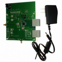
12-Bit 250 Msps ADC EB
Manufacturer
Analog Devices Inc
Datasheet
1.AD9230BCPZ-170.pdf
(32 pages)
Specifications of AD9230-250EBZ
Number Of Adc's
1
Number Of Bits
12
Sampling Rate (per Second)
250M
Data Interface
Serial
Inputs Per Adc
1 Single Ended
Input Range
1.0 ~ 1.5 V
Power (typ) @ Conditions
434mW @ 250MSPS
Voltage Supply Source
Single Supply
Operating Temperature
-40°C ~ 85°C
Utilized Ic / Part
AD9230
Lead Free Status / RoHS Status
Lead free / RoHS Compliant
Lead Free Status / RoHS Status
Lead free / RoHS Compliant


AD9230
CLOCK INPUT CONSIDERATIONS
For optimum performance, the AD9230 sample clock inputs
(CLK+ and CLK−) should be clocked with a differential signal.
This signal is typically ac-coupled into the CLK+ pin and CLK−
pin via a transformer or capacitors. These pins are biased
internally and require no additional bias.
Figure 55 shows one preferred method for clocking the AD9230.
The low jitter clock source is converted from single-ended to
differential using an RF transformer. The back-to-back Schottky
diodes across the secondary transformer limit clock excursions
into the AD9230 to approximately 0.8 V p-p differential. This
helps prevent the large voltage swings of the clock from feeding
through to other portions of the AD9230 and preserves the fast
rise and fall times of the signal, which are critical to low jitter
performance.
If a low jitter clock is available, another option is to ac couple a
differential PECL signal to the sample clock input pins, as
shown in Figure 56. The AD9510/AD9511/AD9512/AD9513/
AD9514/AD9515
performance.
1
50Ω RESISTORS ARE OPTIONAL.
1
CLOCK
CLOCK
50Ω RESISTORS ARE OPTIONAL.
CLOCK
CLOCK
INPUT
INPUT
INPUT
INPUT
CLOCK
INPUT
50Ω
50Ω
1
1
Figure 55. Transformer-Coupled Differential Clock
50Ω
0.1µF
Figure 56. Differential PECL Sample Clock
Figure 57. Differential LVDS Sample Clock
0.1µF
0.1µF
50Ω
0.1µF
0.1µF
50Ω
family of clock drivers offers excellent jitter
1
100Ω
1
CLK
CLK
CLK
CLK
ADT1–1WT, 1:1Z
PECL DRIVER
LVDS DRIVER
MINI-CIRCUITS
AD9510/AD9511/
AD9512/AD9513/
AD9514/AD9515
AD9510/AD9511/
AD9512/AD9513/
AD9514/AD9515
XFMR
0.1µF
240Ω
0.1µF
0.1µF
SCHOTTKY
HSM2812
DIODES:
240Ω
100Ω
100Ω
0.1µF
0.1µF
0.1µF
0.1µF
CLK+
CLK–
AD9230
ADC
CLK+
CLK–
CLK+
CLK–
AD9230
AD9230
ADC
ADC
Rev. 0 | Page 22 of 32
In some applications, it is acceptable to drive the sample clock
inputs with a single-ended CMOS signal. In such applications,
CLK+ should be directly driven from a CMOS gate, and the
CLK− pin should be bypassed to ground with a 0.1 μF capacitor
in parallel with a 39 kΩ resistor (see Figure 58). Although the
CLK+ input circuit supply is AVDD (1.8 V), this input is
designed to withstand input voltages up to 3.3 V, making the
selection of the drive logic voltage very flexible.
Clock Duty Cycle Considerations
Typical high speed ADCs use both clock edges to generate a
variety of internal timing signals. As a result, these ADCs may
be sensitive to clock duty cycle. Commonly, a 5% tolerance is
required on the clock duty cycle to maintain dynamic performance
characteristics. The AD9230 contains a duty cycle stabilizer (DCS)
that retimes the nonsampling edge, providing an internal clock
signal with a nominal 50% duty cycle. This allows a wide range
of clock input duty cycles without affecting the performance of
the AD9230. When the DCS is on, noise and distortion perfor-
mance are nearly flat for a wide range of duty cycles. However,
some applications may require the DCS function to be off. If so,
keep in mind that the dynamic range performance can be affected
when operated in this mode. See the AD9230 Configuration
Using the SPI section for more details on using this feature.
The duty cycle stabilizer uses a delay-locked loop (DLL) to
create the nonsampling edge. As a result, any changes to the
sampling frequency require approximately eight clock cycles
to allow the DLL to acquire and lock to the new rate.
CLOCK
1
1
INPUT
CLOCK
50Ω RESISTOR IS OPTIONAL.
50Ω RESISTOR IS OPTIONAL.
INPUT
Figure 58. Single-Ended 1.8 V CMOS Sample Clock
Figure 59. Single-Ended 3.3 V CMOS Sample Clock
0.1µF
50Ω
0.1µF
50Ω
0.1µF
0.1µF
1
1
CLK
CLK
CMOS DRIVER
CLK
CLK
CMOS DRIVER
AD9510/AD9511/
AD9512/AD9513/
AD9514/AD9515
AD9510/AD9511/
AD9512/AD9513/
AD9514/AD9515
0.1µF
OPTIONAL
OPTIONAL
100Ω
100Ω
39kΩ
0.1µF
0.1µF
0.1µF
CLK+
CLK–
CLK+
CLK–
AD9230
AD9230
ADC
ADC
Related parts for AD9230-250EBZ
Image
Part Number
Description
Manufacturer
Datasheet
Request
R

Part Number:
Description:
12-Bit 170 Msps ADC EB
Manufacturer:
Analog Devices Inc
Datasheet:
Part Number:
Description:
12-Bit 210 Msps ADC EB
Manufacturer:
Analog Devices Inc
Datasheet:

Part Number:
Description:
±1.7g Dual-Axis IMEMS Accelerometer Evaluation Board
Manufacturer:
Analog Devices Inc
Datasheet:
Part Number:
Description:
Inertial Sensor Evaluation System
Manufacturer:
Analog Devices Inc
Datasheet:
Part Number:
Description:
Manufacturer:
Analog Devices Inc
Datasheet:
Part Number:
Description:
Manufacturer:
Analog Devices Inc
Datasheet:
Part Number:
Description:
Manufacturer:
Analog Devices Inc
Datasheet:
Part Number:
Description:
Manufacturer:
Analog Devices Inc
Datasheet:
Part Number:
Description:
Manufacturer:
Analog Devices Inc
Datasheet:
Part Number:
Description:
Manufacturer:
Analog Devices Inc
Datasheet:
Part Number:
Description:
Manufacturer:
Analog Devices Inc
Datasheet:
Part Number:
Description:
Manufacturer:
Analog Devices Inc
Datasheet:
Part Number:
Description:
Manufacturer:
Analog Devices Inc
Datasheet: