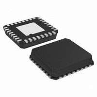
AD9245BCPZ-65 Analog Devices Inc, AD9245BCPZ-65 Datasheet - Page 22

AD9245BCPZ-65
Manufacturer Part Number
AD9245BCPZ-65
Description
IC,A/D CONVERTER,SINGLE,14-BIT,CMOS,LLCC,32PIN
Manufacturer
Analog Devices Inc
Datasheet
1.AD9245BCPZ-80.pdf
(32 pages)
Specifications of AD9245BCPZ-65
Number Of Bits
14
Sampling Rate (per Second)
65M
Data Interface
Parallel
Number Of Converters
3
Power Dissipation (max)
300mW
Voltage Supply Source
Single Supply
Operating Temperature
-40°C ~ 85°C
Mounting Type
Surface Mount
Package / Case
32-VFQFN, CSP Exposed Pad
Lead Free Status / RoHS Status
Lead free / RoHS Compliant
For Use With
AD9245BCP-80EBZ - BOARD EVAL FOR AD9245BCP-80AD9245BCP-40EBZ - BOARD EVAL FOR AD9245BCP-40AD9245BCP-20EBZ - BOARD EVAL FOR AD9245BCP-20
Lead Free Status / RoHS Status
Lead free / RoHS Compliant
AD9245
EXTERNAL REFERENCE OPERATION
The use of an external reference can be necessary to enhance
the gain accuracy of the ADC or improve thermal drift char-
acteristics. When multiple ADCs track one another, a single
reference (internal or external) can be necessary to reduce
gain matching errors to an acceptable level. Figure 48 shows
the typical drift characteristics of the internal reference in both
1.0 V and 0.5 V modes.
When the SENSE pin is tied to AVDD, the internal reference is
disabled, allowing the use of an external reference. An internal
reference buffer loads the external reference with an equivalent
7 kΩ load. The internal buffer still generates the positive and
negative full-scale references, REFT and REFB, for the ADC
core. The input span is always twice the value of the reference
voltage; therefore, the external reference must be limited to a
maximum of 1.0 V.
10μF
+
1.0
0.9
0.8
0.7
0.6
0.5
0.4
0.3
0.2
0.1
0
–40
0.1μF
–30
Figure 47. Programmable Reference Configuration
–20
R2
SENSE
R1
VREF
VIN+
VIN–
–10
Figure 48. Typical VREF Drift
0
TEMPERATURE (°C)
SELECT
LOGIC
10
VREF = 1.0V
VREF = 0.5V
20
AD9245
30
0.5V
CORE
ADC
40
50
REFT
REFB
60
0.1μF
0.1μF
0.1μF
70
80
+
10μF
Rev. D | Page 22 of 32
OPERATIONAL MODE SELECTION
As discussed earlier, the AD9245 can output data in either
offset binary or twos complement format. There is also a
provision for enabling or disabling the clock DCS. The
MODE pin is a multilevel input that controls the data format
and DCS state. The input threshold values and corresponding
mode selections are outlined in Table 11.
Table 11. Mode Selection
MODE Voltage
AVDD
2/3 AVDD
1/3 AVDD
AGND (Default)
EVALUATION BOARD
The AD9245 evaluation board provides the support circuitry
required to operate the ADC in its various modes and
configurations. Complete schematics and layout plots follow
and demonstrate the proper routing and grounding techniques
that should be applied at the system level.
It is critical that signal sources with very low phase noise
(<1 ps rms jitter) be used to realize the ultimate performance of
the converter. Proper filtering of the input signal, to remove
harmonics and lower the integrated noise at the input, is also
necessary to achieve the specified noise performance.
The AD9245 can be driven single-ended or differentially
through a transformer. Separate power pins are provided to
isolate the DUT from the support circuitry. Each input
configuration can be selected by proper connection of
various jumpers (refer to the schematics).
An alternative differential analog input path using an
AD8351 op amp is included in the layout but is not populated
in production. Designers interested in evaluating the op amp
with the ADC should remove C15, R12, and R3 and populate
the op amp circuit. The passive network between the AD8351
outputs and the AD9245 allows the user to optimize the
frequency response of the op amp for the application.
Data Format
Twos Complement
Twos Complement
Offset Binary
Offset Binary
Duty Cycle Stabilizer
Disabled
Enabled
Enabled
Disabled


