AD9430BSV-170 Analog Devices Inc, AD9430BSV-170 Datasheet - Page 13
AD9430BSV-170
Manufacturer Part Number
AD9430BSV-170
Description
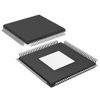
IC,A/D CONVERTER,SINGLE,12-BIT,BICMOS,TQFP,100PIN
Manufacturer
Analog Devices Inc
Datasheet
1.AD9430BSVZ-210.pdf
(44 pages)
Specifications of AD9430BSV-170
Rohs Status
RoHS non-compliant
Number Of Bits
12
Sampling Rate (per Second)
170M
Data Interface
Parallel
Number Of Converters
1
Power Dissipation (max)
1.43mW
Voltage Supply Source
Single Supply
Operating Temperature
-40°C ~ 85°C
Mounting Type
Surface Mount
Package / Case
100-TQFP Exposed Pad
Lead Free Status / RoHS Status
Available stocks
Company
Part Number
Manufacturer
Quantity
Price
Company:

Part Number:
AD9430BSV-170
Manufacturer:
AD
Quantity:
2
Company:
Part Number:
AD9430BSV-170
Manufacturer:
ADI
Quantity:
118
Part Number:
AD9430BSV-170
Manufacturer:
ADI/亚德诺
Quantity:
20 000


Table 8. LVDS Mode Pin Function Descriptions
Pin Number
1
2, 42 to 46
3
4, 9, 12, 13, 16, 17, 20, 23, 25, 26, 30, 31, 35, 38, 41, 86, 87, 91,
92, 93, 96, 97, 100
5
6
7
8, 14, 15, 18, 19, 24, 27, 28, 29, 33, 34, 39, 40, 88, 89, 90, 94, 95,
98, 99
10
11
21
LVDSBIAS
NOTES
1. THE AD9430 HAS A CONDUCTIVE HEAT SLUG TO HELP DISSIPATE HEAT AND ENSURE RELIABLE OPERATION OF
SENSE
THE DEVICE OVER THE FULL INDUSTRIAL TEMPERATURE RANGE. THE SLUG IS EXPOSED ON THE BOTTOM OF
THE PACKAGE AND ELECTRICALLY CONNECTED TO CHIP GROUND. IT IS RECOMMENDED THAT NO PCB SIGNAL
TRACES OR VIAS BE LOCATED UNDER THE PACKAGE THAT COULD COME IN CONTACT WITH THE CONDUCTIVE
SLUG. ATTACHING THE SLUG TO A GROUND PLANE WILL REDUCE THE JUNCTION TEMPERATURE OF THE
DEVICE WHICH MAY BE BENEFICIAL IN HIGH TEMPERATURE ENVIRONMENTS.
AGND
AGND
AGND
AGND
AGND
AGND
AGND
AGND
AGND
AVDD
AVDD
AVDD
AVDD
AVDD
AVDD
VREF
VIN+
VIN–
DNC
S5
S4
S2
S1
10
12
13
14
16
17
19
20
22
23
25
11
15
18
21
24
1
4
2
3
5
6
7
8
9
26 27 28 29 30 31 32 33 34 35 36 37 38 39 40 41 42 43 44 45 46 47 48 49 50
100
PIN 1
99
98
97
96
95
94
Figure 5. LVDS Mode Pin Configuration
93
92
91
Rev. E | Page 13 of 44
90
LVDS PINOUT
(Not to Scale)
Mnemonic
S5
DNC
S4
AGND
S2
S1
LVDSBIAS
AVDD
SENSE
VREF
VIN+
AD9430
TOP VIEW
89
88
2
1
87
86
85
Description
Full-Scale Adjust Pin. AVDD sets f
GND sets f
Do Not Connect.
Control Pin for CMOS Mode. Tie low when operating in LVDS
mode.
Analog Ground.
Output Mode Select. GND = dual-port CMOS; AVDD = LVDS.
Data Format Select. GND = binary, AVDD = twos complement.
Set Pin for LVDS Output Current. Place 3.74 kW resistor
terminated to ground.
3.3 V Analog Supply.
Reference Mode Select Pin. Float for internal reference
operation.
1.235 V Reference I/O—Function Dependent on SENSE.
Analog Input—True.
84
83
82
81
S
= 1.536 V p-p differential.
80
79
78
77
76
75
74
73
72
71
70
69
68
67
66
65
64
63
62
61
60
59
58
57
56
55
54
53
52
51
DRVDD
DRGND
D8+
D8–
D7+
D7–
D6+
D6–
DRGND
D5+
D5–
DCO+
DCO–
DRVDD
DRGND
D4+
D4–
D3+
D3–
D2+
D2Ð
DRVDD
DRGND
D1+
D1–
S
= 0.768 V p-p differential,
AD9430
Related parts for AD9430BSV-170
Image
Part Number
Description
Manufacturer
Datasheet
Request
R


Part Number:
Description:
±1.7g Dual-Axis IMEMS Accelerometer Evaluation Board
Manufacturer:
Analog Devices Inc
Datasheet:

Part Number:
Description:
Inertial Sensor Evaluation System
Manufacturer:
Analog Devices Inc
Datasheet:
Part Number:
Description:
Manufacturer:
Analog Devices Inc
Datasheet:
Part Number:
Description:
Manufacturer:
Analog Devices Inc
Datasheet:
Part Number:
Description:
Manufacturer:
Analog Devices Inc
Datasheet:
Part Number:
Description:
Manufacturer:
Analog Devices Inc
Datasheet:
Part Number:
Description:
Manufacturer:
Analog Devices Inc
Datasheet:
Part Number:
Description:
Manufacturer:
Analog Devices Inc
Datasheet:
Part Number:
Description:
Manufacturer:
Analog Devices Inc
Datasheet:
Part Number:
Description:
Manufacturer:
Analog Devices Inc
Datasheet:
Part Number:
Description:
Manufacturer:
Analog Devices Inc
Datasheet:
Part Number:
Description:
Manufacturer:
Analog Devices Inc
Datasheet: