AD9882KSTZ-140 Analog Devices Inc, AD9882KSTZ-140 Datasheet - Page 30

AD9882KSTZ-140
Manufacturer Part Number
AD9882KSTZ-140
Description
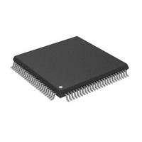
IC,TV/VIDEO CIRCUIT,Video Digitizer,CMOS,QFP,100PIN,PLASTIC
Manufacturer
Analog Devices Inc
Datasheet
1.AD9882KSTZ-100.pdf
(40 pages)
Specifications of AD9882KSTZ-140
Applications
Video
Interface
Analog, DVI
Voltage - Supply
3.15 V ~ 3.45 V
Package / Case
100-LQFP
Mounting Type
Surface Mount
Lead Free Status / RoHS Status
Lead free / RoHS Compliant
Available stocks
Company
Part Number
Manufacturer
Quantity
Price
Company:
Part Number:
AD9882KSTZ-140
Manufacturer:
ADI
Quantity:
717
Company:
Part Number:
AD9882KSTZ-140
Manufacturer:
Analog Devices Inc
Quantity:
10 000
AD9882A
0x11 1 Coast Input Polarity
This bit indicates the polarity of the coast signal that is applied
to the PLL coast input.
This register can be used only when coast is disabled and
Register 0x11, Bit 2 is set to 1.
Table 31. Coast Input Polarity Settings
CSTPOL
0
1
The power-up default value is CSTPOL = 1.
0x12 7–0
This register allows the coast signal to be applied prior to the
Vsync signal. This is necessary in cases where pre-equalization
pulses are present. This register defines the number of edges
that are filtered before Vsync on a composite sync.
The default is 0.
0x13 7–0 Postcoast
This register allows the coast signal to be applied following the
Vsync signal. This is necessary in cases where postequalization
pulses are present. The step size for this control is one Hsync
period. This register defines the number of edges that are
filtered after Vsync on a composite sync.
The default is 0.
0x14 7–6 Output Drive
These two bits select the drive strength for the high speed
digital outputs (all data output and clock output pins). Higher
drive strength results in faster rise/fall times, and in general
makes it easier to capture data. Lower drive strength results in
slower rise/fall times and helps reduce EMI and digitally
generated power supply noise.
Table 32. Output Drive Strength Settings
Bit 7
1
0
0
The default for this register is 11, high drive strength. This
option works on both the analog and digital interfaces.
0x14 5
These bits select the analog bandwidth.
Table 33. Analog Bandwidth Control
Bit 5
0
1
Programmable Analog Bandwidth
Bit 6
X
1
0
Precoast
Result
High drive strength
Medium drive strength
Low drive strength
Function
Active low
Active high
Analog Bandwidth
10 MHz
300 MHz
Rev. 0 | Page 30 of 40
0x14 4
A control bit for the inversion of the output data clock (Pin 85).
This function works only for the digital interface. When not
inverted, data is output on the falling edge of the data clock. See
the Timing Diagrams sections, Figure 14 and Figure 15, to see
how this affects timing.
Table 34. Clock Output Invert Settings
Clk Inv
0
1
The default for this register is 0 (not inverted).
0x14 3
This bit is used to put the outputs in a high impedance mode.
This applies to the 24 data output pins, HSOUT, VSOUT, and
DE pins.
Table 35. Power-Down Output Settings
PDO
0
1
The default for this register is 0. (This option works on both the
analog and digital interfaces.)
0x14 2
This bit is used to set the HDCP slave port address.
Table 36. HDCP Address Settings
Address Bit
0
1
The default for this register is 0.
0x14 1
This bit is used to control chip power-down. See the Power
Management section for details about which blocks are actually
powered down.
Table 37. Power-Down Settings
Select
0
1
The default for this register is 1.
Clk Inv Data Output Clock Invert
PDO Power-Down Outputs
HDCP Address
PWRDN
Function
Normal operation
Three-state
Not inverted
Inverted
Function
Result
Power-down
Normal operation
Result
0 for HDCP Slave Port
1 for HDCP Slave Port


