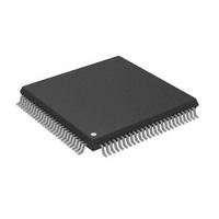
AD9882KSTZ-140 Analog Devices Inc, AD9882KSTZ-140 Datasheet - Page 36

AD9882KSTZ-140
Manufacturer Part Number
AD9882KSTZ-140
Description
IC,TV/VIDEO CIRCUIT,Video Digitizer,CMOS,QFP,100PIN,PLASTIC
Manufacturer
Analog Devices Inc
Datasheet
1.AD9882KSTZ-100.pdf
(40 pages)
Specifications of AD9882KSTZ-140
Applications
Video
Interface
Analog, DVI
Voltage - Supply
3.15 V ~ 3.45 V
Package / Case
100-LQFP
Mounting Type
Surface Mount
Lead Free Status / RoHS Status
Lead free / RoHS Compliant
Available stocks
Company
Part Number
Manufacturer
Quantity
Price
Company:
Part Number:
AD9882KSTZ-140
Manufacturer:
ADI
Quantity:
717
Company:
Part Number:
AD9882KSTZ-140
Manufacturer:
Analog Devices Inc
Quantity:
10 000
AD9882A
PCB LAYOUT RECOMMENDATIONS
The AD9882A is a high precision, high speed analog device. To
derive the maximum performance from the part, it is important
to have a well laid out board. The following is a guide for
designing a board using the AD9882A.
ANALOG INTERFACE INPUTS
Using the following layout techniques on the graphics inputs is
extremely important.
Minimize the trace length running into the graphics inputs.
This is accomplished by placing the AD9882A as close as
possible to the graphics VGA connector. Long input trace
lengths are undesirable because they will pick up more noise
from the board and other external sources.
Place the 75 Ω termination resistors (see Figure 9) as close to
the AD9882A chip as possible. Any additional trace length
between the termination resistors and the input of the
AD9882A increases the magnitude of reflections, which
corrupts the graphics signal.
Use 75 Ω matched impedance traces. Trace impedances other
than 75 Ω also increase the chance of reflections.
The AD9882A has a very high input bandwidth (300 MHz).
While this is desirable for acquiring a high resolution PC
graphics signal with fast edges, it means that it captures any
high frequency noise present. Therefore, it is important to
reduce the amount of noise that gets coupled to the inputs.
Avoid running any digital traces near the analog inputs.
Due to the high bandwidth of the AD9882A, sometimes low-
pass filtering the analog inputs can help to reduce noise. (For
many applications, filtering is unnecessary.) Experiments have
shown that placing a series ferrite bead prior to the 75 Ω
termination resistor is helpful in filtering out excess noise.
Specifically, the part used was the #2508051217Z0 from Fair-
Rite, but different applications may work best with different
bead values. Alternatively, placing a 100 Ω to 120 Ω resistor
between the 75 Ω termination resistor and the input coupling
capacitor can also be beneficial.
DIGITAL INTERFACE INPUTS
Many of the same techniques that are recommended for the
analog interface inputs should also be used for the digital
interface inputs. It is important to minimize trace lengths, then
make the input trace impedances match the input termination
(typically 50 Ω). Each differential input pair (R
R
routing techniques and should be kept as short as possible. No
other components, such as clamping diodes, should be placed
on these inputs. Every effort should be made to route these
signals on a single layer (component layer) with no vias.
XC–
, and so on) should be routed together using 50 Ω strip line
X0+
, R
X0–
, R
XC+
,
Rev. 0 | Page 36 of 40
POWER SUPPLY BYPASSING
Bypassing each power supply pin with a 0.1 µF capacitor is
recommended. The exception is when two or more supply pins
are adjacent to each other. For these groupings of powers/
grounds, it is necessary to have one bypass capacitor. The
fundamental idea is to have a bypass capacitor within about 0.5
cm of each power pin. Also, avoid placing the capacitor on the
side of the PC board opposite the AD9882A, as that interposes
resistive vias in the path.
The bypass capacitors should be physically located between the
power plane and the power pin. Current should flow from the
power plane ->to the capacitor ->to the power pin. Do not
make the power connection between the capacitor and the
power pin. Placing a via underneath the capacitor pads, down
to the power plane, is generally the best approach.
It is particularly important to maintain low noise and good
stability of PV
PV
phase and frequency. This can be avoided by careful attention to
regulation, filtering, and bypassing. It is highly desirable to
provide separate regulated supplies for each of the analog
circuitry groups (V
Some graphic controllers use levels of power when active
(during active picture time) that are substantially different from
those used when they are idle (during horizontal and vertical
sync periods). This can result in a measurable change in the
voltage supplied to the analog supply regulator, which can in
turn produce changes in the regulated analog supply voltage.
This can be mitigated by regulating the analog supply, or at least
PV
a 12 V supply).
Using a single ground plane for the entire board is also recom-
mended. Experience has repeatedly shown that the noise
performance is the same or better with a single ground plane.
Using multiple ground planes can be detrimental, because each
separate ground plane is smaller than one common ground
plane, and can result in long ground loops.
In some cases, using separate ground planes is unavoidable.
When they must be used, it is recommended that at least a
single ground plane be placed under the AD9882A. The
location of the split should be at the receiver of the digital
outputs. In this case, it is even more important to place
components wisely, because the current loops are much longer
(current takes the path of least resistance). The following is an
example of a current loop: power plane -> AD9882A -> digital
output trace -> digital data receiver -> digital ground plane ->
analog ground plane.
D
D
, from a different, cleaner, power source (for example, from
can result in similarly abrupt changes in sampling clock
D
(the clock generator supply). Abrupt changes in
D
and PV
D
).


