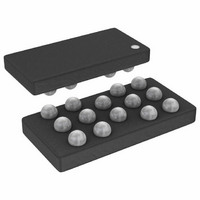
ADA4505-4ACBZ-R7 Analog Devices Inc, ADA4505-4ACBZ-R7 Datasheet - Page 14

ADA4505-4ACBZ-R7
Manufacturer Part Number
ADA4505-4ACBZ-R7
Description
Quad 10uA CMOS/Zero Crossover Amp-AD8508
Manufacturer
Analog Devices Inc
Datasheet
1.ADA4505-2ACBZ-R7.pdf
(20 pages)
Specifications of ADA4505-4ACBZ-R7
Amplifier Type
Voltage Feedback
Number Of Circuits
4
Output Type
Rail-to-Rail
Slew Rate
0.006 V/µs
Gain Bandwidth Product
50kHz
Current - Input Bias
0.5pA
Voltage - Input Offset
500µV
Current - Supply
7µA
Current - Output / Channel
40mA
Voltage - Supply, Single/dual (±)
1.8 V ~ 5 V, ±0.9 V ~ 2.5 V
Operating Temperature
-40°C ~ 125°C
Mounting Type
Surface Mount
Package / Case
14-WLCSP
Lead Free Status / RoHS Status
Lead free / RoHS Compliant
-3db Bandwidth
-
Lead Free Status / RoHS Status
Lead free / RoHS Compliant
Other names
ADA4505-4ACBZ-R7TR
Available stocks
Company
Part Number
Manufacturer
Quantity
Price
Company:
Part Number:
ADA4505-4ACBZ-R7
Manufacturer:
AD
Quantity:
9 195
ADA4505-2/ADA4505-4
THEORY OF OPERATION
The ADA4505-2/ADA4505-4 are unity-gain stable CMOS rail-
to-rail input/output operational amplifiers designed to optimize
performance in current consumption, PSRR, CMRR, and zero
crossover distortion, all embedded in a small package. The typical
offset voltage is 500 μV, with a low peak-to-peak voltage noise
of 2.95 μV from 0.1 Hz to 10 Hz and a voltage noise density of
65 nV/√Hz at 1 kHz.
The ADA4505-2/ADA4505-4 are designed to solve two key
problems in low voltage battery-powered applications: battery
voltage decrease over time and rail-to-rail input stage distortion.
In battery-powered applications, the supply voltage available to
the IC is the voltage of the battery. Unfortunately, the voltage of
a battery decreases as it discharges itself through the load. This
voltage drop over the lifetime of the battery causes an error in
the output of the op amps. Some applications requiring precision
measurements during the entire lifetime of the battery use
voltage regulators to power up the op amps as a solution. If a
design uses standard battery cells, the op amps experience a
supply voltage change from roughly 3.2 V to 1.8 V during the
lifetime of the battery. This means that for a PSRR of 70 dB
minimum in a typical op amp, the input-referred offset error
is approximately 440 μV. If the same application uses the
ADA4505-2/ADA4505-4 with a 100 dB minimum PSRR, the
error is only 14 μV. It is possible to calibrate this error out or
to use an external voltage regulator to power the op amp, but
these solutions can increase system cost and complexity. The
ADA4505-2/ADA4505-4 solve the impasse with no additional
cost or error-nullifying circuitry.
The second problem with battery-powered applications is the
distortion caused by the standard rail-to-rail input stage. Using
a CMOS non-rail-to-rail input stage (that is, a single differential
pair) limits the input voltage to approximately one V
source voltage) away from one of the supply lines. Because V
for normal operation is commonly over 1 V, a single differential
pair input stage op amp greatly restricts the allowable input
voltage range when using a low supply voltage. This limitation
restricts the number of applications where the non-rail-to-rail
input op amp was originally intended to be used. To solve this
problem, a dual differential pair input stage is usually implemented
(see Figure 49); however, this technique has its own drawbacks.
One differential pair amplifies the input signal when the common-
mode voltage is on the high end, whereas the other pair amplifies
the input signal when the common-mode voltage is on the low
end. This method also requires control circuitry to operate the
two differential pairs appropriately. Unfortunately, this topology
leads to a very noticeable and undesirable problem; if the signal
level moves through the range where one input stage turns off and
the other one turns on, noticeable distortion occurs (see Figure 50).
GS
(gate-
Rev. B | Page 14 of 20
GS
This distortion forces the designer to devise impractical ways
to avoid the crossover distortion areas, thereby narrowing the
common-mode dynamic range of the operational amplifier. The
ADA4505-2/ADA4505-4 solve this crossover distortion problem
by using an on-chip charge pump to power the input differential
pair. The charge pump creates a supply voltage higher than the
voltage of the battery, allowing the input stage to handle a wide
range of input signal voltages without using a second differential
pair. With this solution, the input voltage can vary from one
supply extreme to the other with no distortion, thereby restoring
the full common-mode dynamic range of the op amp.
(Dual PMOS Q1 and Q2 Transistors Form the Lower End of the Input Voltage
Response in a Dual Differential Pair Input Stage Op Amp (Powered by 5 V
Supply; Results of Approximately 100 Units per Graph Are Displayed)
Figure 50. Typical Input Offset Voltage vs. Common-Mode Voltage
I
V
B
Range; Dual NMOS Q3 and Q4 Transistors Form the Upper End)
–100
–150
–200
–250
–300
IN+
300
250
200
150
100
–50
Figure 49. Typical Dual Differential Pair Input Stage Op Amp
50
0
V
0
SS
Q3
V
T
0.5
SY
A
= 25°C
= 5V
Q1
1.0
1.5
Q2
2.0
V
CM
V
Q4
2.5
DD
(V)
3.0
V
IN–
I
B
3.5
4.0
4.5
V
BIAS
5.0


