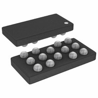
ADA4505-4ACBZ-R7 Analog Devices Inc, ADA4505-4ACBZ-R7 Datasheet - Page 15

ADA4505-4ACBZ-R7
Manufacturer Part Number
ADA4505-4ACBZ-R7
Description
Quad 10uA CMOS/Zero Crossover Amp-AD8508
Manufacturer
Analog Devices Inc
Datasheet
1.ADA4505-2ACBZ-R7.pdf
(20 pages)
Specifications of ADA4505-4ACBZ-R7
Amplifier Type
Voltage Feedback
Number Of Circuits
4
Output Type
Rail-to-Rail
Slew Rate
0.006 V/µs
Gain Bandwidth Product
50kHz
Current - Input Bias
0.5pA
Voltage - Input Offset
500µV
Current - Supply
7µA
Current - Output / Channel
40mA
Voltage - Supply, Single/dual (±)
1.8 V ~ 5 V, ±0.9 V ~ 2.5 V
Operating Temperature
-40°C ~ 125°C
Mounting Type
Surface Mount
Package / Case
14-WLCSP
Lead Free Status / RoHS Status
Lead free / RoHS Compliant
-3db Bandwidth
-
Lead Free Status / RoHS Status
Lead free / RoHS Compliant
Other names
ADA4505-4ACBZ-R7TR
Available stocks
Company
Part Number
Manufacturer
Quantity
Price
Company:
Part Number:
ADA4505-4ACBZ-R7
Manufacturer:
AD
Quantity:
9 195
The charge pump has been carefully designed so that switching
noise components at any frequency, both within and beyond the
amplifier bandwidth, are much lower than the thermal noise floor.
Therefore, the spurious-free dynamic range (SFDR) is limited
only by the input signal and the thermal or flicker noise. There
is no intermodulation between input signal and switching noise.
Figure 51 displays a typical front-end section of an operational
amplifier with an on-chip charge pump.
Figure 52 shows the typical response of two devices from Figure 10,
which shows the input offset voltage vs. input common-mode
voltage for 10 devices. Figure 52 is expanded to make it easier to
compare with Figure 50, which shows the typical input offset
voltage vs. common-mode voltage response in a dual differential
pair input stage op amp.
V
BIAS
V
+IN
PP
Figure 51. Typical Front-End Section of an Op Amp
V
PP
Q1
= POSITIVE PUMPED VOLTAGE = V
with Embedded Charge Pump
Q2
–IN
V
V
DD
SS
RAIL-TO-RAIL
CASCODE
OUTPUT
STAGE
STAGE
AND
DD
+ 1.8V
OUT
Rev. B | Page 15 of 20
This solution improves the CMRR performance tremendously.
For example, if the input varies from rail to rail on a 2.5 V
supply rail, using a part with a CMRR of 70 dB minimum,
an input-referred error of 790 μV is introduced. Another part
with a CMRR of 52 dB minimum generates a 6.3 mV error.
The ADA4505-2/ADA4505-4 CMRR of 90 dB minimum causes
only a 79 μV error. As with the PSRR error, there are complex
ways to minimize this error, but the ADA4505-2/ADA4505-4
solve this problem without incurring unnecessary circuitry
complexity or increased cost.
Figure 52. Input Offset Voltage vs. Input Common-Mode Voltage Response
–100
–150
–200
–250
–300
(Powered by a 5 V Supply; Results of Two Units Are Displayed)
300
250
200
150
100
–50
50
0
0
V
T
SY
A
0.5
= 25°C
= 5V
1.0
1.5
ADA4505-2/ADA4505-4
2.0
V
CM
2.5
(V)
3.0
3.5
4.0
4.5
5.0


