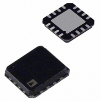
ADG1433YCPZ-REEL7 Analog Devices Inc, ADG1433YCPZ-REEL7 Datasheet - Page 7

ADG1433YCPZ-REEL7
Manufacturer Part Number
ADG1433YCPZ-REEL7
Description
IC,ANALOG SWITCH,TRIPLE,SPDT,CMOS,LLCC,16PIN,PLASTIC
Manufacturer
Analog Devices Inc
Series
iCMOS®r
Type
Analog Switchr
Datasheet
1.ADG1434YCPZ-REEL7.pdf
(20 pages)
Specifications of ADG1433YCPZ-REEL7
Function
Switch
Circuit
3 x SPDT
On-state Resistance
4.7 Ohm
Voltage Supply Source
Dual, Single, Dual Supply
Voltage - Supply, Single/dual (±)
±5V, 12V, ±15V
Current - Supply
1µA
Operating Temperature
-40°C ~ 125°C
Mounting Type
Surface Mount
Package / Case
16-VQFN, CSP Exposed Pad
Multiplexer Configuration
Triple SPDT
Number Of Inputs
3
Number Of Outputs
6
Number Of Channels
3
Analog Switch On Resistance
9@±4.5VOhm
Analog Switch Turn On Time
425ns
Analog Switch Turn Off Time
200ns
Package Type
LFCSP
Power Supply Requirement
Single/Dual
Single Supply Voltage (min)
5V
Single Supply Voltage (typ)
12V
Single Supply Voltage (max)
16.5V
Dual Supply Voltage (min)
±4.5V
Dual Supply Voltage (typ)
±5/±15V
Dual Supply Voltage (max)
±16.5V
Supply Current
0.26mA
Mounting
Surface Mount
Pin Count
16
Operating Temp Range
-40C to 125C
Operating Temperature Classification
Automotive
Package
16LFCSP EP
Maximum On Resistance
9@±4.5V Ohm
Maximum Propagation Delay Bus To Bus
430@±5V|255@12V|170@±15V ns
Maximum Turn-off Time
200@±5V ns
Maximum Turn-on Time
425@±5V ns
Switch Architecture
SPDT
Power Supply Type
Single|Dual
Lead Free Status / RoHS Status
Lead free / RoHS Compliant
Lead Free Status / RoHS Status
Lead free / RoHS Compliant
Other names
ADG1433YCPZ-REEL7TR
Available stocks
Company
Part Number
Manufacturer
Quantity
Price
Company:
Part Number:
ADG1433YCPZ-REEL7
Manufacturer:
ADI
Quantity:
12 821
ABSOLUTE MAXIMUM RATINGS
T
Table 4.
Parameter
V
V
V
Analog Inputs, Digital Inputs
Peak Current, S or D (Pulsed at 1 ms,
Continuous Current, S or D
Operating Temperature Range
Junction Temperature
Reflow Soldering Peak
1
2
Stresses above those listed under Absolute Maximum Ratings
may cause permanent damage to the device. This is a stress
rating only; functional operation of the device at these or any
other conditions above those indicated in the operational
section of this specification is not implied. Exposure to absolute
maximum rating conditions for extended periods may affect
device reliability.
Only one absolute maximum rating may be applied at any
one time.
Overvoltages at A, EN , S, or D pins are clamped by internal diodes. Current
should be limited to the maximum ratings given.
See data given in the Specifications section (see Table 1 to Table 3).
DD
DD
SS
A
Industrial (Y Version)
Storage Temperature Range
10% Duty Cycle Maximum)
Temperature (Pb-Free)
= 25°C, unless otherwise noted.
to GND
to V
to GND
SS
2
1
Rating
35 V
−0.3 V to +25 V
−25 V to +0.3 V
V
30 mA, whichever occurs first
250 mA
Data + 15%
−40°C to +125°C
−65°C to +150°C
150°C
260 (+ 0 to −5)°C
SS
− 0.3 V to V
DD
+ 0.3 V or
Rev. C | Page 7 of 20
THERMAL RESISTANCE
θ
soldered in a circuit board for surface-mount packages.
Table 5.
Package Type
TSSOP
LFCSP_VQ
ESD CAUTION
JA
is specified for the worst-case conditions, that is, a device
θ
150.4
30.4
JA
ADG1433/ADG1434
θ
50
N/A
JC
Unit
°C/W
°C/W


