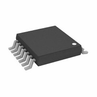
ADG604YRUZ-REEL7 Analog Devices Inc, ADG604YRUZ-REEL7 Datasheet - Page 5

ADG604YRUZ-REEL7
Manufacturer Part Number
ADG604YRUZ-REEL7
Description
IC,ANALOG MUX,QUAD,1-CHANNEL,CMOS,TSSOP,14PIN,PLASTIC
Manufacturer
Analog Devices Inc
Type
Analog Multiplexerr
Datasheet
1.ADG604YRUZ.pdf
(12 pages)
Specifications of ADG604YRUZ-REEL7
Function
Multiplexer
Circuit
1 x 4:1
On-state Resistance
115 Ohm
Voltage Supply Source
Dual Supply
Voltage - Supply, Single/dual (±)
±2.7 V ~ 5.5 V
Current - Supply
0.001µA
Operating Temperature
-40°C ~ 85°C
Mounting Type
Surface Mount
Package / Case
14-TSSOP (0.173", 4.40mm Width)
Package
14TSSOP
Maximum On Resistance
460@2.7V Ohm
Maximum Propagation Delay Bus To Bus
100@±5V|150@5V|320@3V ns
Maximum High Level Output Current
10 mA
Multiplexer Architecture
4:1
Maximum Turn-off Time
160@3V ns
Maximum Turn-on Time
250@3V ns
Power Supply Type
Single|Dual
Lead Free Status / RoHS Status
Lead free / RoHS Compliant
ABSOLUTE MAXIMUM RATINGS
(T
V
V
V
Analog Inputs
Digital Inputs
Peak Current, S or D . . . . . . . . . . . . . . . . . . . . . . . . . . 20 mA
Continuous Current, S or D . . . . . . . . . . . . . . . . . . . . 10 mA
Operating Temperature Range
Storage Temperature Range . . . . . . . . . . . . –65°C to +150°C
CAUTION
ESD (electrostatic discharge) sensitive device. Electrostatic charges as high as 4000 V readily
accumulate on the human body and test equipment and can discharge without detection. Although
the ADG604 features proprietary ESD protection circuitry, permanent damage may occur on
devices subjected to high-energy electrostatic discharges. Therefore, proper ESD precautions are
recommended to avoid performance degradation or loss of functionality.
DD
DD
SS
(Pulsed at 1 ms, 10% Duty Cycle Max)
Automotive (Y Version) . . . . . . . . . . . . . . –40°C to +125°C
A
. . . . . . . . . . . . . . . . . . . . . . 30 mA, Whichever Occurs First
= 25°C unless otherwise noted)
to GND . . . . . . . . . . . . . . . . . . . . . . . . . +0.3 V to –6.5 V
to V
to GND . . . . . . . . . . . . . . . . . . . . . . . . –0.3 V to +6.5 V
SS
. . . . . . . . . . . . . . . . . . . . . . . . . . . . . . . . . . . . 13 V
2
2
Model Option
ADG604YRU
. . . . . . . . . . . . . . . . V
. . . . . . . . . . . . . . . . . –0.3 V to V
PIN CONFIGURATION
V
NC
EN
A0
S1
S2
SS
D
NC = NO CONNECT
1
2
3
4
5
6
7
(Not To Scale)
ADG604
TOP VIEW
Temperature Range
–40°C to +125°C
1
14
13
12
11
10
9
8
SS
A1
GND
V
S3
S4
NC
NC
–0.3 V to V
DD
DD
DD
+ 0.3 V or
+ 0.3 V
ORDERING GUIDE
Package Description
Thin Shrink Small Outline (TSSOP)
Junction Temperature . . . . . . . . . . . . . . . . . . . . . . . . . 150°C
TSSOP Package
Lead Temperature, Soldering (10 seconds) . . . . . . . . . 300°C
NOTES
1
2
Stresses above those listed under Absolute Maximum Ratings may cause perma-
Overvoltages at EN, A0, A1, S, or D will be clamped by internal diodes. Current
nent damage to the device. This is a stress rating only; functional operation of the
device at these or any other conditions above those listed in the operational
sections of this specification is not implied. Exposure to absolute maximum rating
conditions for extended periods may affect device reliability. Only one absolute
maximum rating may be applied at any one time.
should be limited to the maximum ratings given.
IR Reflow, Peak Temperature . . . . . . . . . . . . . . . . . 220°C
JA
JC
Thermal Impedance . . . . . . . . . . . . . . . . . . . . 150°C/W
Thermal Impedance . . . . . . . . . . . . . . . . . . . . . 27°C/W
A1
X
0
0
1
1
Table I. Truth Table
A0
X
0
1
0
1
EN
0
1
1
1
1
WARNING!
Package
RU-14
ON Switch
None
1
2
3
4
ESD SENSITIVE DEVICE
ADG604


