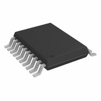
ADG936BRU Analog Devices Inc, ADG936BRU Datasheet - Page 4

ADG936BRU
Manufacturer Part Number
ADG936BRU
Description
WBand Absorbtive/Reflve Dual SPDT IC
Manufacturer
Analog Devices Inc
Datasheet
1.EVAL-ADG936EBZ.pdf
(16 pages)
Specifications of ADG936BRU
Rf Type
General Purpose
Frequency
0Hz ~ 2GHz
Features
SPDT
Package / Case
20-TSSOP
Frequency (max)
2GHz
Insertion Loss (max)
1.25dB
Number Of Switches
Dual
Pin Count
20
Package Type
TSSOP
Lead Free Status / RoHS Status
Contains lead / RoHS non-compliant
Lead Free Status / RoHS Status
Contains lead / RoHS non-compliant, Contains lead / RoHS non-compliant
Available stocks
Company
Part Number
Manufacturer
Quantity
Price
Part Number:
ADG936BRU
Manufacturer:
ADI/亚德诺
Quantity:
20 000
Part Number:
ADG936BRU-R
Manufacturer:
ADI/亚德诺
Quantity:
20 000
Part Number:
ADG936BRUZ
Manufacturer:
ADI/亚德诺
Quantity:
20 000
Part Number:
ADG936BRUZ-R
Manufacturer:
ADI/亚德诺
Quantity:
20 000
ADG936/ADG936-R
ABSOLUTE MAXIMUM RATINGS
T
Table 2.
Parameter
V
Inputs to GND
Continuous Current
Input Power
Operating Temperature Range
Storage Temperature Range
Junction Temperature
TSSOP Package
LFCSP Package
Lead Temperature, Soldering (10 sec)
IR Reflow, Peak Temperature (<20 sec)
ESD
ESD CAUTION
ESD (electrostatic discharge) sensitive device. Electrostatic charges as high as 4000 V readily accumulate on
the human body and test equipment and can discharge without detection. Although this product features
proprietary ESD protection circuitry, permanent damage may occur on devices subjected to high energy
electrostatic discharges. Therefore, proper ESD precautions are recommended to avoid performance
degradation or loss of functionality.
DD
A
Industrial (B Version)
θ
θ
= 25°C, unless otherwise noted.
to GND
JA
JA
Thermal Impedance (4-Layer Board)
Thermal Impedance
Rating
–0.5 V to +4 V
–0.5 V to V
30 mA
18 dBm
–40°C to +85°C
–65°C to +150°C
150°C
143°C/W
30.4°C/W
300°C
235°C
1 kV
DD
+ 0.3 V
Rev. A | Page 4 of 16
1
Stresses above those listed under Absolute Maximum Ratings
may cause permanent damage to the device. This is a stress
rating only; functional operation of the device at these or any
other conditions above those indicated in the operational
section of this specification is not implied. Exposure to absolute
maximum rating conditions for extended periods may affect
device reliability.
Only one absolute maximum rating may be applied at any one
time.
Table 3. Truth Table
INx
0
1
1
RF1x/RF2x off port inputs to ground = –0.5 V to V
RF1x
Off
On
DD
– 0.5 V.
RF2x
On
Off


