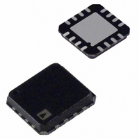
ADN2525ACPZ-R2 Analog Devices Inc, ADN2525ACPZ-R2 Datasheet

ADN2525ACPZ-R2
Specifications of ADN2525ACPZ-R2
ADN2525ACPZ-R2TR
Related parts for ADN2525ACPZ-R2
ADN2525ACPZ-R2 Summary of contents
Page 1
FEATURES Up to 10.7 Gbps operation Very low power: 670 mW (IBIAS = 40 mA, IMOD = 40 mA) Typical 24 ps rise/fall times Full back-termination of output transmission lines Compatible with XMD-MSA TOSA Drives TOSAs with resistances ranging from ...
Page 2
ADN2525 TABLE OF CONTENTS Features .............................................................................................. 1 Applications....................................................................................... 1 General Description ......................................................................... 1 Functional Block Diagram .............................................................. 1 Revision History ............................................................................... 2 Specifications..................................................................................... 3 Thermal Specifications ................................................................ 4 Absolute Maximum Ratings............................................................ 5 ESD Caution.................................................................................. 5 Pin Configuration and Function Descriptions............................. ...
Page 3
SPECIFICATIONS VCC = VCC to VCC , T = −40°C to +85°C, 50 Ω differential load resistance, unless otherwise noted. Typical values are specified at MIN MAX A 25°C, IMOD = 40 mA. Table 1. Parameter BIAS CURRENT (IBIAS) Bias ...
Page 4
ADN2525 1 Refers to the voltage between the pin for which the compliance voltage is specified and GND. 2 The pattern used is composed by a repetitive sequence of eight 1s followed by eight 0s at 10.7 Gbps. 3 Measured ...
Page 5
ABSOLUTE MAXIMUM RATINGS Table 3. Parameter Min Supply Voltage, VCC to GND −0.3 IMODP, IMODN to GND VCC − DATAP, DATAN to GND VCC − 1.8 All Other Pins −0.3 Junction Temperature Storage Temperature Range −65 Soldering Temperature ...
Page 6
ADN2525 PIN CONFIGURATION AND FUNCTION DESCRIPTIONS Note that the exposed pad on the bottom of the package must be connected to the VCC or GND plane. Table 4. Pin Function Description Pin No. Mnemonic 1 MSET ALS ...
Page 7
TYPICAL PERFORMANCE CHARACTERISTICS T = 25°C, VCC = 3.3 V, unless otherwise noted. A 28.0 27.5 27.0 26.5 26.0 25.5 25.0 24.5 24.0 23.5 23 DIFFERENTIAL MODULATION CURRENT (mA) Figure 5. Rise Time vs. IMOD 27.5 ...
Page 8
ADN2525 0 –5 –10 –15 –20 –25 –30 –35 – FREQUENCY (GHz) Figure 11. Differential |S22 ...
Page 9
THEORY OF OPERATION As shown in Figure 1, the ADN2525 consists of an input stage and two voltage-controlled current sources for bias and modulation. The bias current is available at the IBIAS pin controlled by the voltage at ...
Page 10
ADN2525 The equivalent circuits of the BSET, IBIAS, and IBMON pins are shown in Figure 20, Figure 21, and Figure 22. VCC VCC BSET 800Ω 200Ω Figure 20. Equivalent Circuit of the BSET Pin IBIAS VCC VCC 100Ω 2Ω Figure ...
Page 11
No portion of the modulation current flows in the active back- termination resistance. All of the preset modulation current IMOD, the range specified in Table 1, ...
Page 12
ADN2525 IMODP, IMODN VCC + 1.1V NORMAL OPERATION REGION VCC VCC – 1.1V Figure 30. Allowable Range for the Voltage at IMODP and IMODN LOAD MISTERMINATION Due to its excellent S22 performance, the ADN2525 can drive differential loads that range ...
Page 13
APPLICATIONS INFORMATION TYPICAL APPLICATION CIRCUIT Figure 33 shows the typical application circuit for the ADN2525. The dc voltages applied to the BSET and MSET pins control the bias and modulation currents. The bias current can be monitored as a voltage ...
Page 14
ADN2525 DESIGN EXAMPLE This design example covers: • Headroom calculations for IBIAS, IMODP, and IMODN pins. • Calculation of the typical voltage required at the BSET and MSET pins to produce the desired bias and modulation currents. This design example ...
Page 15
... OUTLINE DIMENSIONS PIN 1 INDICATOR 12° MAX 0.90 0.85 0.80 SEATING PLANE ORDERING GUIDE Model Temperature Range ADN2525ACPZ-WP 1 −40°C to +85°C 1 ADN2525ACPZ-R2 −40°C to +85°C 1 ADN2525ACPZ-REEL7 −40°C to +85° Pb-free part. 3.00 0.60 MAX BSC SQ 0. 2.75 TOP BSC SQ ...
Page 16
ADN2525 NOTES ©2006 Analog Devices, Inc. All rights reserved. Trademarks and registered trademarks are the property of their respective owners. D05077-0-8/06(A) T Rev Page ...


