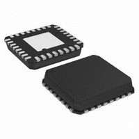
ADN2841ACPZ-32 Analog Devices Inc, ADN2841ACPZ-32 Datasheet

ADN2841ACPZ-32
Specifications of ADN2841ACPZ-32
Available stocks
Related parts for ADN2841ACPZ-32
ADN2841ACPZ-32 Summary of contents
Page 1
FEATURES 50 Mbps to 2.7 Gbps Operation Typical Rise/Fall Time 80 ps Bias Current Range 2 to 100 mA Modulation Current Range Monitor Photodiode Current 1200 A Closed-Loop Control of Power and ...
Page 2
ADN2841–SPECIFICATIONS Parameter LASER BIAS (BIAS) Output Current I BIAS Compliance Voltage I during ALS BIAS ALS Response Time CCBIAS Compliance Voltage MODULATION CURRENT (IMODP, IMODN) Output Current I MOD Compliance Voltage I during ALS MOD Rise Time Fall Time Jitter ...
Page 3
Parameter IBMON, IMMON, IMPDMON, IMPDMON2 IBMON, IMMON Division Ratio IMPDMON, IMPDMON2 IMPDMON to IMPDMON2 Matching Compliance Voltage SUPPLY NOTES 1 Temperature range: –40°C to +85°C. 2 When the voltage on DATAP is greater than ...
Page 4
ADN2841 48-Lead LFCSP GND2 37 VCC2 38 IMODN 39 IMODN 40 GND2 41 ADN2841 IMODP 42 TOP VIEW IMODP 43 (Not to Scale) GND2 44 GND2 45 IBIAS 46 IBIAS 47 CCBIAS 48 PIN 1 INDICATOR Pin No. 48-Lead 32-Lead ...
Page 5
Pin No. 48-Lead 32-Lead Mnemonic 37 GND2 38 25 VCC2 39 26 IMODN 40 IMODN 41 27 GND2 42 28 IMODP 43 IMODP 44 29 GND2 45 30 GND2 46 31 IBIAS 47 IBIAS 48 32 CCBIAS REV. A PIN ...
Page 6
ADN2841 GENERAL Laser diodes have current-in to light-out transfer functions as shown in Figure 2. Two key characteristics of this transfer function are the threshold current and the slope in the linear region beyond TH the threshold current, ...
Page 7
REF CLOCK 20MHz– 180MHz CLKIN 1.25mA–20mA I OUT AD9850/AD9851 DDS I OUT R SET 50 37.5 A–600 A CONTROLLER The second photodiode current is mirrored to IMPDMON2 for wavelength control purposes and is summed internally for the power control loop. ...
Page 8
ADN2841 ALARM INTERFACES A 30 kΩ internal pull-up resistor is employed to pull the digital high value of the alarm outputs However, the ADN2841 CC has a feature that allows the user to externally wire resistors in ...
Page 9
SHOULD HAVE BYPASS CAPACITORS AS CLOSE AS POSSIBLE TO THE CC ACTUAL SUPPLY PINS ON THE ADN2841 AND THE LASER DIODE USED. Figure 7. Anyrate Test Circuit, Capacitively Coupled, Data ...
Page 10
ADN2841 MODULATOR GND LBWSET ASET V ERSET CC PSET GND IMPD IMPDMON IMPDMON2 IMPD2 GND4 VCC4 12 Figure 9. Unfiltered 2.5 Gbps Optical Eye. Average Power = –3 dBm, Extinction Ratio = 9.5 ...
Page 11
PIN 1 INDICATOR 1.00 12 MAX 0.90 0.80 0.25 REF SEATING PLANE PIN 1 INDICATOR 12 MAX 1.00 0.90 0.80 SEATING PLANE REV. A OUTLINE DIMENSIONS 48-Lead Frame Chip Scale Package [LFCSP] (CP-48) Dimensions shown in millimeters 7.00 BSC SQ ...
Page 12
Revision History Location 8/02—Data Sheet changed from REV REV. A. Figure 8 replaced . . . . . . . . . . . . . . . . . . . . . . . . . ...


