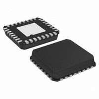
ADN2841ACPZ-32-RL7 Analog Devices Inc, ADN2841ACPZ-32-RL7 Datasheet - Page 6

ADN2841ACPZ-32-RL7
Manufacturer Part Number
ADN2841ACPZ-32-RL7
Description
IC,Laser Diode/LED Driver,LLCC,32PIN,CERAMIC
Manufacturer
Analog Devices Inc
Type
Laser Diode Driver (Fiber Optic)r
Datasheet
1.ADN2841ACPZ-32.pdf
(12 pages)
Specifications of ADN2841ACPZ-32-RL7
Data Rate
2.7Gbps
Number Of Channels
1
Voltage - Supply
4.5 V ~ 5.5 V
Current - Supply
50mA
Current - Modulation
80mA
Current - Bias
100mA
Operating Temperature
-40°C ~ 85°C
Package / Case
32-VFQFN, CSP Exposed Pad
Mounting Type
Surface Mount
Lead Free Status / RoHS Status
Lead free / RoHS Compliant
ADN2841
GENERAL
Laser diodes have current-in to light-out transfer functions as shown
in Figure 2. Two key characteristics of this transfer function are the
threshold current, I
the threshold current, referred to as slope efficiency, LI.
CONTROL
A monitor photodiode (MPD) is required to control the LD. The
MPD current is fed into the ADN2841 to control the optical
power and extinction ratio, continuously adjusting the bias current
and modulation current in response to the laser’s changing
threshold current and light-to-current (LI) slope (slope efficiency).
The ADN2841 uses automatic power control (APC) to main-
tain a constant power over time and temperature.
The ADN2841 uses closed-loop extinction ratio control to allow
optimum setting of extinction ratio for every device. Therefore,
SONET/SDH interface standards can be met over device varia-
tion, temperature, and time. Closed-loop modulation control
eliminates the need to either overmodulate the LD or include
external components for temperature compensation. This reduces
research and development time and second-sourcing issues
caused by characterizing LDs.
Average power and extinction ratio are set using the PSET and
ERSET pins, respectively. Potentiometers are connected between
these pins and ground. The potentiometer R
change the average power. The potentiometer R
to adjust the extinction ratio. Both PSET and ERSET are
kept 1.23 V above GND.
R
where I
where P
sheet, I
P
Note that I
However, the control loops will determine actual values. It is not
required to know the exact values for LI or MPD optical coupling.
AV
PSET
is the required average power.
and R
MPD_CW
AV
CW
is the average MPD current.
R
is the dc optical power specified on the laser data
ERSET
ERSET
ERSET
Figure 2. Laser Transfer Function
is the MPD current at that specified P
P
P1
P0
AV
and I
can be calculated using the following formulas:
=
TH
I
ER =
P
, and the slope in the linear region beyond
MPD CW
PSET
AV
P
R
=
CW
PSET
P1
P0
–
P1 + P0
will change from device to device.
2
=
×
1 23
1 23
ER
ER
.
I
.
I
TH
AV
−
+
V
V
1
1
I
CURRENT
×
P
0 2
.
LI =
PSET
×
P
P
ERSET
I
AV
is used to
CW
is used
, and
–6–
LOOP BANDWIDTH SELECTION
For anyrate operation, the user should hardwire the LBWSET
pin high and use 1 µF capacitors to set the actual loop band-
width. These capacitors are placed between the PAVCAP and
ERCAP pins and ground. It is important that these capacitors
be low leakage multilayer ceramics with an insulation resistance
greater than 100 GΩ or a time constant of 1000 sec, whichever
is less. The ADN2841 may be optimized for 2.7 Gbps operation
by keeping the LBWSET pin low. This results in a much shorter
loop time constant (a 10 reduction). The value of PAVCAP
and ERCAP capacitors required for 2.5 Gbps operation is 22 nF.
ALARMS
The ADN2841 alarms are designed to allow interface compliance
to ITU-T-G958 (11/94) section 10.3.1.1.2 (transmitter fail) and
section 10.3.1.1.3 (transmitter degrade). The ADN2841 has
two active high alarms, DEGRADE and FAIL. A resistor between
ground and the ASET pin is used to set the current at which
these alarms are raised. The current through the ASET resistor is
a ratio of 100:1 to the FAIL alarm threshold. The DEGRADE
alarm will be raised at 90% of this level.
Example:
NOTE: The smallest value for R
sponds to the I
The laser degrade alarm, DEGRADE, gives a warning of imminent
laser failure if the laser diode degrades further or environmental
conditions, e.g., increasing temperature, continue to stress the LD.
The laser fail alarm, FAIL, is activated when the transmitter can
no longer be guaranteed to be SONET/SDH compliant. This
occurs when one of the following conditions arises:
DEGRADE will only be raised when the bias current exceeds
90% of ASET current.
MONITOR CURRENTS
IBMON, IMMON, IMPDMON, and IMPDMON2 are
current controlled current sources from V
bias, modulation, and MPD current for increased monitoring
functionality. An external resistor to GND gives a voltage
proportional to the current monitored.
DUAL MPD DWDM FUNCTION (48-LEAD LFCSP ONLY)
The ADN2841 has circuitry for an optional second monitor
photodiode, MPD2.
• The ASET threshold is reached.
• The ALS pin is set high. This shuts off the modulation and
bias currents to the LD, resulting in the MPD current
dropping to zero. This gives closed-loop feedback to the
system in which ALS has been enabled.
R
I
I
ASET
BIAS
ASET
FAIL
maximum of 100 mA.
=
=
=
50
I
1 23
BIASTRIP
I
.
100
ASET
mA
V
∴
=
I
=
500
DEGRADE
1 23
ASET
50
.
100
µ
mA
is 1.2 kΩ, as this corre-
V
A
=
=
=
CC
2 46
45
500
. They mirror the
.
mA
µ
k
A
Ω
REV. A


