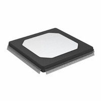
ADSP-21061LASZ-176 Analog Devices Inc, ADSP-21061LASZ-176 Datasheet - Page 18

ADSP-21061LASZ-176
Manufacturer Part Number
ADSP-21061LASZ-176
Description
ADSP-21061l 44 Mhz 3v
Manufacturer
Analog Devices Inc
Series
SHARC®r
Type
Floating Pointr
Datasheet
1.ADSP-21061LKSZ-160.pdf
(56 pages)
Specifications of ADSP-21061LASZ-176
Interface
Synchronous Serial Port (SSP)
Clock Rate
44MHz
Non-volatile Memory
External
On-chip Ram
128kB
Voltage - I/o
3.30V
Voltage - Core
3.30V
Operating Temperature
-40°C ~ 85°C
Mounting Type
Surface Mount
Package / Case
240-MQFP, 240-PQFP
Lead Free Status / RoHS Status
Lead free / RoHS Compliant
Available stocks
Company
Part Number
Manufacturer
Quantity
Price
Company:
Part Number:
ADSP-21061LASZ-176
Manufacturer:
Analog Devices Inc
Quantity:
10 000
ADSP-21061/ADSP-21061L
ADSP-21061L SPECIFICATIONS
OPERATING CONDITIONS (3.3 V)
1
2
ELECTRICAL CHARACTERISTICS (3.3 V)
1
2
3
4
5
6
7
8
9
10
11
Applies to input and bidirectional pins: DATA
Applies to input pins: CLKIN, RESET, TRST
Applies to output and bidirectional pins: DATA
See “Output Drive Currents” for typical drive current capabilities.
Applies to input pins: ACK, SBTS, IRQ
Applies to input pins with internal pull-ups: DR0, DR1, TRST, TMS, TDI, EMU.
Applies to three-statable pins: DATA
Applies to three-statable pins with internal pull-ups: DT0, DT1, TCLK0, TCLK1, RCLK0, RCLK1.
Applies to CPA pin.
Applies to ACK pin when pulled up. (Note that ACK is pulled up internally with 2 kΩ during reset in a multiprocessor system, when ID
Applies to ACK pin when keeper latch enabled.
Applies to all signal pins.
Guaranteed but not tested.
Parameter
V
T
V
V
V
Parameter
V
V
I
I
I
I
I
I
I
I
I
I
C
TFS1, RFS0, RFS1, EBOOT, BMS, TMS, TDI, TCK, HBR, DR0, DR1, TCLK0, TCLK1, RCLK0, RCLK1
BR
TDO, EMU. (Note that ACK is pulled up internally with 2 kΩ during reset in a multiprocessor system, when ID
mastership.)
is not requesting bus mastership).
IH
IL
ILP
OZH
OZL
OZHP
OZLC
OZLA
OZLAR
OZLS
CASE
DD
IH
IH
IL
OH
OL
IN
3
3, 4
4
1
2
6–1
10, 11
1, 2
5
1, 2
1,2
5, 6, 7, 8
6
7
9
1
2
8
, CPA, DT0, DT1, TCLK0, TCLK1, RCLK0, RCLK1, TFS0, TFS1, RFS0, RFS1, BMS, TDO, EMU, ICSA.
Description
Supply Voltage
Case Operating Temperature
High Level Input Voltage @ V
High Level Input Voltage @ V
Low Level Input Voltage @ V
Description
High Level Output Voltage
Low Level Output Voltage
High Level Input Current
Low Level Input Current
Low Level Input Current
Three-State Leakage Current
Three-State Leakage Current
Three-State Leakage Current
Three-State Leakage Current
Three-State Leakage Current
Three-State Leakage Current
Three-State Leakage Current
Input Capacitance
47–0
2–0
, ADDR
, HBR, CS, DMAR1, DMAR2, ID
47–0
47–0
31–0
, ADDR
, ADDR
, MS
3–0
31–0
DD
DD
DD
31–0
, RD, WR, PAGE, ADRCLK, SW, ACK, FLAG
= Min
, RD, WR, SW , ACK, SBTS, IRQ2–0, FLAG3–0, HGB, CS, DMAR1, DMAR2, BR
= Max
= Max
, 3-0, MS
Rev. C | Page 18 of 56 | July 2007
3–0
, RD, WR, PAGE, ADRCLK, SW, ACK, FLAG3-0, TIMEXP, HBG, REDY, DMAG1, DMAG2,
2–0
, RPBA, EBOOT, LBOOT, CLKIN, RESET, TCK.
Test Conditions
@ V
@ V
@ V
@ V
@ V
@ V
@ V
@ V
@ V
@ V
@ V
@ V
f
IN
= 1 MHz, T
DD
DD
DD
DD
DD
DD
DD
DD
DD
DD
DD
DD
= Min, I
= Min, I
= Max, V
= Max, V
= Max, V
= Max, V
= Max, V
= Max, V
= Max, V
= Max, V
= Max, V
= Max, V
Min
3.15
–40
2.0
2.2
–0.5
CASE
OH
OL
IN
IN
IN
IN
IN
IN
IN
IN
IN
IN
= 4.0 mA
= –2.0 mA
= V
= 0 V
= 0 V
= V
= 0 V
= V
= 0 V
= 1.5 V
= 0 V
= 0 V
= 25°C, V
DD
DD
DD
A Grade
3–0
Max
Max
Max
, HBG, REDY, DMAG1, DMAG2, BMS, BR
Max
3.45
+85
V
V
+0.8
IN
DD
DD
2–0
= 2.5 V
+ 0.5
+ 0.5
= 001 and another ADSP-21061 is not requesting bus
Min
3.15
0
2.0
2.2
–0.5
2–0
Min
2.4
= 001 and another ADSP-21061L
K Grade
6–1
, ID
Max
3.45
+85
V
V
+0.8
DD
DD
2–0
Max
0.4
10
10
150
10
10
350
1.5
350
4.2
150
4.7
+ 0.5
+ 0.5
, RPBA, CPA, TFS0,
6–1
, TFSx, RFSx,
Unit
V
V
μA
μA
μA
μA
μA
μA
mA
μA
mA
μA
pF
Unit
V
°C
V
V
V


