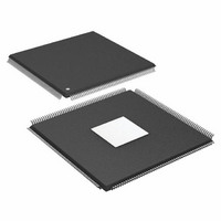
ADSP-21369BSWZ-2A Analog Devices Inc, ADSP-21369BSWZ-2A Datasheet - Page 42

ADSP-21369BSWZ-2A
Manufacturer Part Number
ADSP-21369BSWZ-2A
Description
333 MHz, Shared Memory,S/PDIF EPAD PBfr
Manufacturer
Analog Devices Inc
Series
SHARC®r
Type
Floating Pointr
Datasheet
1.ADSP-21369KBPZ-2A.pdf
(60 pages)
Specifications of ADSP-21369BSWZ-2A
Interface
DAI, DPI
Clock Rate
333MHz
Non-volatile Memory
ROM (768 kB)
On-chip Ram
256kB
Voltage - I/o
3.30V
Voltage - Core
1.20V
Operating Temperature
-40°C ~ 85°C
Mounting Type
Surface Mount
Package / Case
208-LQFP
Device Core Size
32/40Bit
Architecture
Super Harvard
Format
Floating Point
Clock Freq (max)
333MHz
Mips
333
Device Input Clock Speed
333MHz
Ram Size
256KB
Program Memory Size
768KB
Operating Supply Voltage (typ)
1.2/3.3V
Operating Supply Voltage (min)
1.14/3.13V
Operating Supply Voltage (max)
1.26/3.47V
Operating Temp Range
-40C to 85C
Operating Temperature Classification
Industrial
Mounting
Surface Mount
Pin Count
208
Package Type
LQFP EP
Package
208LQFP EP
Numeric And Arithmetic Format
Floating-Point
Maximum Speed
333 MHz
Device Million Instructions Per Second
333 MIPS
Lead Free Status / RoHS Status
Lead free / RoHS Compliant
Lead Free Status / RoHS Status
Lead free / RoHS Compliant
Available stocks
Company
Part Number
Manufacturer
Quantity
Price
Company:
Part Number:
ADSP-21369BSWZ-2A
Manufacturer:
Analog Devices Inc
Quantity:
10 000
ADSP-21367/ADSP-21368/ADSP-21369
S/PDIF Transmitter
Serial data input to the S/PDIF transmitter can be formatted as
left justified, I
or 24 bits. The following sections provide timing for the
transmitter.
Figure 31
for the left channel and high for the right channel. Data is valid
on the rising edge of SCLK. The MSB is left-justified to an
LRCLK transition but with a single SCLK period delay.
Figure 32
left channel and low for the right channel. Data is valid on the
rising edge of SCLK. The MSB is left-justified to an LRCLK
transition with no MSB delay.
DAI_P20–1
DAI_P20–1
DAI_P20–1
DAI_P20–1
DAI_P20–1
DAI_P20–1
LRCLK
SDATA
SCLK
SDATA
LRCLK
SCLK
DAI_P20–1
DAI_P20–1
DAI_P20–1
LRCLK
SDATA
SCLK
shows the default I
shows the left-justified mode. LRCLK is high for the
2
S, or right justified with word widths of 16, 18, 20,
LSB
MSB
MSB – 1
MSB – 2
MSB
2
MSB – 1
S-justified mode. LRCLK is low
MSB – 2
LSB + 2
MSB
LEFT CHANNEL
MSB – 1
LEFT CHANNEL
LSB + 1
LSB + 2
MSB – 2
LSB
LEFT CHANNEL
LSB + 1
Rev. E | Page 42 of 60 | July 2009
Figure 30. Right-Justified Mode
Figure 32. Left-Justified Mode
LSB
LSB + 2
Figure 31. I
LSB + 1
LSB
2
S-Justified Mode
MSB
MSB – 1
RIGHT CHANNEL
S/PDIF Transmitter—Serial Input Waveforms
Figure 30
left channel and low for the right channel. Data is valid on the
rising edge of SCLK. The MSB is delayed 12-bit clock periods
(in 20-bit output mode) or 16-bit clock periods (in 16-bit output
mode) from an LRCLK transition, so that when there are 64
SCLK periods per LRCLK period, the LSB of the data is right-
justified to the next LRCLK transition.
MSB – 2
MSB
MSB – 1
MSB – 2
shows the right-justified mode. LRCLK is high for the
RIGHT CHANNEL
RIGHT CHANNEL
LSB + 2
MSB
MSB – 1
LSB + 1
MSB – 2
LSB + 2
LSB
LSB + 1
LSB
LSB + 2
LSB + 1
LSB
MSB
MSB + 1
MSB


