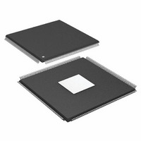
ADSP-21369BSWZ-2A Analog Devices Inc, ADSP-21369BSWZ-2A Datasheet - Page 44

ADSP-21369BSWZ-2A
Manufacturer Part Number
ADSP-21369BSWZ-2A
Description
333 MHz, Shared Memory,S/PDIF EPAD PBfr
Manufacturer
Analog Devices Inc
Series
SHARC®r
Type
Floating Pointr
Datasheet
1.ADSP-21369KBPZ-2A.pdf
(60 pages)
Specifications of ADSP-21369BSWZ-2A
Interface
DAI, DPI
Clock Rate
333MHz
Non-volatile Memory
ROM (768 kB)
On-chip Ram
256kB
Voltage - I/o
3.30V
Voltage - Core
1.20V
Operating Temperature
-40°C ~ 85°C
Mounting Type
Surface Mount
Package / Case
208-LQFP
Device Core Size
32/40Bit
Architecture
Super Harvard
Format
Floating Point
Clock Freq (max)
333MHz
Mips
333
Device Input Clock Speed
333MHz
Ram Size
256KB
Program Memory Size
768KB
Operating Supply Voltage (typ)
1.2/3.3V
Operating Supply Voltage (min)
1.14/3.13V
Operating Supply Voltage (max)
1.26/3.47V
Operating Temp Range
-40C to 85C
Operating Temperature Classification
Industrial
Mounting
Surface Mount
Pin Count
208
Package Type
LQFP EP
Package
208LQFP EP
Numeric And Arithmetic Format
Floating-Point
Maximum Speed
333 MHz
Device Million Instructions Per Second
333 MIPS
Lead Free Status / RoHS Status
Lead free / RoHS Compliant
Lead Free Status / RoHS Status
Lead free / RoHS Compliant
Available stocks
Company
Part Number
Manufacturer
Quantity
Price
Company:
Part Number:
ADSP-21369BSWZ-2A
Manufacturer:
Analog Devices Inc
Quantity:
10 000
ADSP-21367/ADSP-21368/ADSP-21369
S/PDIF Receiver
The following section describes timing as it relates to the
S/PDIF receiver.
Internal Digital PLL Mode
In the internal digital phase-locked loop mode the internal PLL
(digital PLL) generates the 512 × FS clock.
Table 39. S/PDIF Receiver Internal Digital PLL Mode Timing
1
Parameter
Switching Characteristics
t
t
t
t
t
SCLK frequency is 64 × FS where FS = the frequency of LRCLK.
DFSI
HOFSI
DDTI
HDTI
SCLKIW
1
LRCLK Delay After SCLK
LRCLK Hold After SCLK
Transmit Data Delay After SCLK
Transmit Data Hold After SCLK
Transmit SCLK Width
(DATA CHANNEL
DAI_P20–1
DAI_P20–1
DAI_P20–1
(SCLK)
A/B)
(FS)
Figure 34. S/PDIF Receiver Internal Digital PLL Mode Timing
DRIVE EDGE
t
t
HOFSI
Rev. E | Page 44 of 60 | July 2009
HDTI
t
t
DDTI
DFSI
t
SCLKIW
Min
–2
–2
40
SAMPLE EDGE
5
Max
5
Unit
ns
ns
ns
ns
ns


