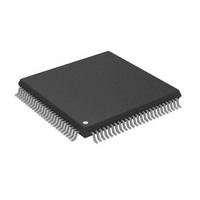
ADSP-2185MKSTZ-300 Analog Devices Inc, ADSP-2185MKSTZ-300 Datasheet - Page 11

ADSP-2185MKSTZ-300
Manufacturer Part Number
ADSP-2185MKSTZ-300
Description
75mhz,16k/16k, 2.5v, Lqfp
Manufacturer
Analog Devices Inc
Series
ADSP-21xxr
Type
Fixed Pointr
Datasheet
1.ADSP-2185MBSTZ-266.pdf
(40 pages)
Specifications of ADSP-2185MKSTZ-300
Interface
Host Interface, Serial Port
Clock Rate
75MHz
Non-volatile Memory
External
On-chip Ram
80kB
Voltage - I/o
3.30V
Voltage - Core
2.50V
Operating Temperature
0°C ~ 70°C
Mounting Type
Surface Mount
Package / Case
100-LQFP
Lead Free Status / RoHS Status
Lead free / RoHS Compliant
Other names
ADSP-2185MKSTZ300
Available stocks
Company
Part Number
Manufacturer
Quantity
Price
Company:
Part Number:
ADSP-2185MKSTZ-300
Manufacturer:
Analog Devices Inc
Quantity:
10 000
Part Number:
ADSP-2185MKSTZ-300
Manufacturer:
ADI/亚德诺
Quantity:
20 000
RESET
The RESET signal initiates a master reset of the ADSP-2185M.
The RESET signal must be asserted during the power-up
sequence to assure proper initialization. RESET during initial
power-up must be held long enough to allow the internal clock
to stabilize. If RESET is activated any time after power-up, the
clock continues to run and does not require stabilization time.
The power-up sequence is defined as the total time required for the
crystal oscillator circuit to stabilize after a valid V
the processor, and for the internal phase-locked loop (PLL) to lock
onto the specific crystal frequency. A minimum of 2000 CLKIN
cycles ensures that the PLL has locked but does not include the
crystal oscillator start-up time. During this power-up sequence
the RESET signal should be held low. On any subsequent resets,
the RESET signal must meet the minimum pulsewidth specifi-
cation, t
The RESET input contains some hysteresis; however, if an
RC circuit is used to generate the RESET signal, the use of an
external Schmidt trigger is recommended.
The master reset sets all internal stack pointers to the empty stack
condition, masks all interrupts, and clears the MSTAT register.
When RESET is released, if there is no pending bus request and
the chip is configured for booting, the boot-loading sequence is
MODE D
X
X
0
0
1
1
NOTE
1
Considered as standard operating settings. Using these configurations allows for easier design and better memory management.
RSP
.
MODE C
0
0
1
1
1
1
CLKIN
DSP
XTAL
MODE B
0
1
0
0
0
0
CLKOUT
MODE A
0
0
0
1
0
1
DD
Table II. Modes of Operation
is applied to
Booting Method
BDMA feature is used to load the first 32 program memory words from
the byte memory space. Program execution is held off until all 32 words
have been loaded. Chip is configured in Full Memory Mode.
No automatic boot operations occur. Program execution starts at external
memory location 0. Chip is configured in Full Memory Mode. BDMA can
still be used, but the processor does not automatically use or wait for these
operations.
BDMA feature is used to load the first 32 program memory words from
the byte memory space. Program execution is held off until all 32 words
have been loaded. Chip is configured in Host Mode. IACK has active
pull-down. (REQUIRES ADDITIONAL HARDWARE).
IDMA feature is used to load any internal memory as desired. Program
execution is held off until internal program memory location 0 is written
to. Chip is configured in Host Mode. IACK has active pull-down.
BDMA feature is used to load the first 32 program memory words from
the byte memory space. Program execution is held off until all 32 words
have been loaded. Chip is configured in Host Mode; IACK requires exter-
nal pull down. (REQUIRES ADDITIONAL HARDWARE)
IDMA feature is used to load any internal memory as desired. Program
execution is held off until internal program memory location 0 is written
to. Chip is configured in Host Mode. IACK requires external pull-down.
performed. The first instruction is fetched from on-chip pro-
gram memory location 0x0000 once boot loading completes.
Power Supplies
The ADSP-2185M has separate power supply connections for
the internal (V
The internal supply must meet the 2.5 V requirement. The
external supply can be connected to either a 2.5 V or 3.3 V supply.
All external supply pins must be connected to the same supply.
All input and I/O pins can tolerate input voltages up to 3.6 V,
regardless of the external supply voltage. This feature provides
maximum flexibility in mixing 2.5 V and 3.3 V components.
MODES OF OPERATION
Setting Memory Mode
Memory Mode selection for the ADSP-2185M is made during
chip reset through the use of the Mode C pin. This pin is multi-
plexed with the DSP’s PF2 pin, so care must be taken in how
the mode selection is made. The two methods for selecting the
value of Mode C are active and passive.
Passive Configuration
Passive Configuration involves the use a pull-up or pull-down
resistor connected to the Mode C pin. To minimize power con-
sumption, or if the PF2 pin is to be used as an output in the DSP
application, a weak pull-up or pull-down, on the order of 10 kΩ,
can be used. This value should be sufficient to pull the pin to the
desired level and still allow the pin to operate as a programmable
flag output without undue strain on the processor’s output driver.
For minimum power consumption during power-down, recon-
figure PF2 to be an input, as the pull-up or pull-down will
hold the pin in a known state, and will not switch.
DDINT
) and external (V
DDEXT
ADSP-2185M
) power supplies.
1
1
1


