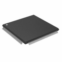
ADSP-2191MBSTZ-140 Analog Devices Inc, ADSP-2191MBSTZ-140 Datasheet - Page 9

ADSP-2191MBSTZ-140
Manufacturer Part Number
ADSP-2191MBSTZ-140
Description
IC,DSP,16-BIT,CMOS,QFP,144PIN,PLASTIC
Manufacturer
Analog Devices Inc
Series
ADSP-21xxr
Type
Fixed Pointr
Specifications of ADSP-2191MBSTZ-140
Interface
Host Interface, SPI, SSP, UART
Clock Rate
140MHz
Non-volatile Memory
External
On-chip Ram
160kB
Voltage - I/o
3.00V, 3.30V
Voltage - Core
2.50V
Operating Temperature
-40°C ~ 85°C
Mounting Type
Surface Mount
Package / Case
144-LQFP
Device Core Size
16b
Clock Freq (max)
140MHz
Mips
140
Device Input Clock Speed
140MHz
Ram Size
160KB
Operating Supply Voltage (typ)
2.5/3.3V
Operating Supply Voltage (min)
2.37/2.97V
Operating Supply Voltage (max)
2.63/3.6V
Operating Temp Range
-40C to 85C
Operating Temperature Classification
Industrial
Mounting
Surface Mount
Pin Count
144
Package Type
LQFP
Lead Free Status / RoHS Status
Lead free / RoHS Compliant
Lead Free Status / RoHS Status
Lead free / RoHS Compliant
Other names
ADSP-2191MBSTZ140
Available stocks
Company
Part Number
Manufacturer
Quantity
Price
Company:
Part Number:
ADSP-2191MBSTZ-140
Manufacturer:
MAXIM
Quantity:
101
Company:
Part Number:
ADSP-2191MBSTZ-140
Manufacturer:
Analog Devices Inc
Quantity:
10 000
• Framing—each transmit and receive port can run with or
• Companding in hardware—each SPORT can perform
• DMA operations with single-cycle overhead—each
• Interrupts—each transmit and receive port generates an
• Multichannel capability—each SPORT supports the
Serial Peripheral Interface (SPI) Ports
The DSP has two SPI-compatible ports that enable the DSP to
communicate with multiple SPI-compatible devices. These ports
are multiplexed with SPORT2, so either SPORT2 or the SPI
ports are active, depending on the state of the OPMODE pin
during hardware reset.
The SPI interface uses three pins for transferring data: two data
pins (Master Output-Slave Input, MOSIx, and Master
Input-Slave Output, MISOx) and a clock pin (Serial Clock,
SCKx). Two SPI chip select input pins (SPISSx) let other SPI
devices select the DSP, and fourteen SPI chip select output pins
(SPIxSEL7–1) let the DSP select other SPI devices. The SPI
select pins are reconfigured Programmable Flag pins. Using
these pins, the SPI ports provide a full duplex, synchronous serial
interface, which supports both master and slave modes and mul-
timaster environments.
Each SPI port’s baud rate and clock phase/polarities are program-
mable (see equation below for SPI clock rate calculation), and
each has an integrated DMA controller, configurable to support
both transmit and receive data streams. The SPI’s DMA control-
ler can only service unidirectional accesses at any given time.
REV. A
without frame sync signals for each data word. Frame sync
signals can be generated internally or externally, active
high or low, and with either of two pulsewidths and early
or late frame sync.
A-law or µ-law companding according to ITU recommen-
dation G.711. Companding can be selected on the
transmit and/or receive channel of the SPORT without
additional latencies.
SPORT can automatically receive and transmit multiple
buffers of memory data, one data word each DSP cycle.
Either the DSP’s core or a Host processor can link or chain
sequences of DMA transfers between a SPORT and
memory. The chained DMA can be dynamically allocated
and updated through the DMA descriptors (DMA
transfer parameters) that set up the chain.
interrupt upon completing the transfer of a data word or
after transferring an entire data buffer or buffers through
DMA.
H.100 standard.
SPI Clock Rate
=
--------------------------------------
2 SPIBAUD
×
HCLK
–9–
During transfers, the SPI ports simultaneously transmit and
receive by serially shifting data in and out on their two serial data
lines. The serial clock line synchronizes the shifting and sampling
of data on the two serial data lines.
UART Port
The UART port provides a simplified UART interface to another
peripheral or Host. It performs full duplex, asynchronous
transfers of serial data. Options for the UART include support
for 5–8 data bits; 1 or 2 stop bits; and none, even, or odd parity.
The UART port supports two modes of operation:
• Programmed I/O
• DMA (direct memory access)
The UART’s baud rate (see following equation for UART clock
rate calculation), serial data format, error code generation and
status, and interrupts are programmable:
• Supported bit rates range from 9.5 bits to 5M bits per
• Supported data formats are 7- to 12-bit frames.
• Transmit and receive status can be configured to generate
The timers can be used to provide a hardware-assisted autobaud
detection mechanism for the UART interface.
Where D is the programmable divisor = 1 to 65536.
Programmable Flag (PFx) Pins
The ADSP-2191M has 16 bidirectional, general-purpose I/O,
Programmable Flag (PF15–0) pins. The PF7–0 pins are
dedicated to general-purpose I/O. The PF15–8 pins serve either
as general-purpose I/O pins (if the DSP is connected to an 8-bit
external data bus) or serve as DATA15–8 lines (if the DSP is
connected to a 16-bit external data bus). The Programmable Flag
pins have special functions for clock multiplier selection and for
SPI port operation. For more information, see
The DSP’s core sends or receives data by writing or
reading I/O-mapped THR or RBR registers, respectively.
The data is double-buffered on both transmit and receive.
The DMA controller transfers both transmit and receive
data. This reduces the number and frequency of inter-
rupts required to transfer data to and from memory. The
UART has two dedicated DMA channels. These DMA
channels have lower priority than most DMA channels
because of their relatively low service rates.
second (80 MHz peripheral clock).
maskable interrupts to the DSP’s core.
UART Clock Rate
ADSP-2191M
=
HCLK
----------------- -
16 D
×
Serial Peripheral


