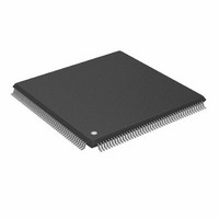
ADSP-21992BSTZ Analog Devices Inc, ADSP-21992BSTZ Datasheet - Page 35

ADSP-21992BSTZ
Manufacturer Part Number
ADSP-21992BSTZ
Description
Mixed Signal DSP W/32K DM RAM& 16K PMRAM
Manufacturer
Analog Devices Inc
Series
ADSP-21xxr
Type
Fixed Pointr
Datasheet
1.ADSP-21992BSTZ.pdf
(60 pages)
Specifications of ADSP-21992BSTZ
Interface
SPI, SSP
Clock Rate
160MHz
Non-volatile Memory
External
On-chip Ram
128kB
Voltage - I/o
3.30V
Voltage - Core
2.50V
Operating Temperature
-40°C ~ 85°C
Mounting Type
Surface Mount
Package / Case
176-LQFP
Lead Free Status / RoHS Status
Lead free / RoHS Compliant
Available stocks
Company
Part Number
Manufacturer
Quantity
Price
Company:
Part Number:
ADSP-21992BSTZ
Manufacturer:
AD
Quantity:
430
Company:
Part Number:
ADSP-21992BSTZ
Manufacturer:
Analog Devices Inc
Quantity:
10 000
External Port Write Cycle Timing
Table 20
The external port lets systems extend read/write accesses in
three ways: wait states, ACK input, and combined wait states
and ACK. To add waits with ACK, the DSP must see ACK low
Table 20. External Port Write Cycle Timing
1
2
3
4
5
6
t
These are timing parameters that are based on worst-case operating conditions.
W = (number of wait states specified in wait register)
Write hold cycle memory select control registers (MS 3 CTL).
Write wait state count (E_WHC) = 0
Write wait state count (E_WHC) = 1
EMICLK
Parameter
Timing Requirements
t
t
Switching Characteristics
t
t
t
t
t
t
t
t
t
t
t
AKW
DWSAK
CSWS
AWS
WSCS
WSA
WW
CDA
CDD
DSW
DHW
DHW
WWR
is the external memory interface clock period. t
and
Figure 10
ACK Strobe Pulse Width
ACK Delay from XMS Low
Chip Select Asserted to WR Asserted Delay
Address Valid to WR Setup and Delay
WR Deasserted to Chip Select Deasserted
WR Deasserted to Address Invalid
Data Valid to WR Deasserted Setup
WR Strobe Pulse Width
WR to Data Enable Access Delay
WR to Data Disable Access Delay
WR Deasserted to Data Invalid Hold Time; E_WHC
WR Deasserted to Data Invalid Hold Time; E_WHC
WR Deasserted to WR, RD Asserted
1, 2
describe external port write operations.
HCLK
t
EMICLK
is the peripheral clock period.
Rev. A | Page 35 of 60 | August 2007
.
4, 5
4, 6
at the rising edge of EMI clock. ACK low causes the DSP to wait,
and the DSP requires two EMI clock cycles after ACK goes high
to finish the access. For more information, see the External Port
chapter in the ADSP-2199x DSP Hardware Reference.
Min
12.5
0.5t
0.5t
0.5t
0.5t
t
0.5t
t
3.4
t
t
EMICLK
EMICLK
EMICLK
HCLK
EMICLK
EMICLK
EMICLK
EMICLK
EMICLK
–2 + W
+3.4
+ 1 + W
– 4
– 3
– 4
– 3
– 3
3
3
Max
0.5t
0
0.5t
t
EMICLK
EMICLK
EMICLK
+ 7 + W
– 1
+ 4
ADSP-21992
3
Unit
ns
ns
ns
ns
ns
ns
ns
ns
ns
ns
ns
ns
ns


