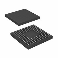
ADSP-BF531SBBC400 Analog Devices Inc, ADSP-BF531SBBC400 Datasheet - Page 21

ADSP-BF531SBBC400
Manufacturer Part Number
ADSP-BF531SBBC400
Description
IC,MICROPROCESSOR,32-BIT,CMOS,BGA,160PIN,PLASTIC
Manufacturer
Analog Devices Inc
Series
Blackfin®r
Type
Fixed Pointr
Datasheet
1.ADSP-BF531SBSTZ400.pdf
(12 pages)
Specifications of ADSP-BF531SBBC400
Rohs Status
RoHS non-compliant
Interface
SPI, SSP, UART
Clock Rate
400MHz
Non-volatile Memory
ROM (1 kB)
On-chip Ram
52kB
Voltage - I/o
1.8V, 2.5V, 3.3V
Voltage - Core
1.20V
Operating Temperature
-40°C ~ 85°C
Mounting Type
Surface Mount
Package / Case
160-CSPBGA
Device Core Size
16b
Architecture
Modified Harvard
Format
Fixed Point
Clock Freq (max)
400MHz
Mips
400
Device Input Clock Speed
400MHz
Operating Supply Voltage (typ)
1.2/1.8/2.5/3.3V
Operating Supply Voltage (min)
0.8/1.75V
Operating Supply Voltage (max)
1.32/3.6V
Operating Temp Range
-40C to 85C
Operating Temperature Classification
Industrial
Mounting
Surface Mount
Pin Count
160
Package Type
CSPBGA
Package
160CSP-BGA
Numeric And Arithmetic Format
Fixed-Point
Maximum Speed
400 MHz
Device Million Instructions Per Second
400 MIPS
For Use With
ADZS-BF533-EZLITE - KIT W/BOARD EVAL FOR ADSP-BF533
Lead Free Status / Rohs Status
Not Compliant
Available stocks
Company
Part Number
Manufacturer
Quantity
Price
Company:
Part Number:
ADSP-BF531SBBC400
Manufacturer:
ADI
Quantity:
329
Company:
Part Number:
ADSP-BF531SBBC400
Manufacturer:
Analog Devices Inc
Quantity:
10 000
Part Number:
ADSP-BF531SBBC400
Manufacturer:
ADI/亚德诺
Quantity:
20 000
Silicon Anomaly List
37.
38.
39.
DESCRIPTION:
When Data CPLBs are enabled, hardware errors generated as a result of speculative accesses to reserved or undefined memory should not
occur, but they do.
WORKAROUND:
None. Avoid accessing reserved memory as part of a speculative fetch.
The VisualDSP++ Blackfin compiler will ignore uses of its '-cplbs' switch when building for silicon revisions that are impacted by this
anomaly or when the switch '-workaround no-cplb-spec-protect-246' is used. Uses of -cplbs would otherwise allow the compiler to ignore
specualtive fetch issues.
APPLIES TO REVISION(S):
0.3, 0.4
DESCRIPTION:
In multichannel mode, when the period of the frame sync is bigger than the actual data frame width by ONE bit (i.e. there is one "inactive
bit"), the FIRST word of the transmitted frame is shifted to the left by one bit and the LSB is the MSB of the second word. All other words
are transmitted correctly.
All data is transmitted correctly if the Frame Sync period is equal to the actual frame width or bigger by more than 1 bit.
For example, if there are 8 words of 16-bit data each, that would be 128 bits in the data frame.
If RFSDIV = 127 --> all data words are CORRECT
If RFSDIV = 128 --> first word is INCORRECT
If RFSDIV = 129 --> all data words are CORRECT
If RFSDIV = 130 --> all data words are CORRECT
WORKAROUND:
Set the RFSDIV register value to the number of data bits +/- 1 to avoid the case described above.
APPLIES TO REVISION(S):
0.4
DESCRIPTION:
The General-Purpose Timers can generate PWM output waveforms on the TMRx pin whose timing is quantified in either system clock
(SCLK) periods or in periods of an externally supplied clock (TMRCLK or TACLK). For proper operation, SCLK must be faster than the source
that is utilized, TMRCLK or TACLK.
The specification in the data sheet and hardware reference manual allows for TMRCLK and TACLK speeds of up to 1/2 SCLK.
However, the maximum rate is less than this limit. The minimum SCLK/TMRCLK or SCLK/TACLK ratio is somewhere in the range of 2.5 to
2.7. The exact value is not yet characterized.
WORKAROUND:
A minimum SCLK/TMRCLK or SCLK/TACLK ratio of 3 is safe to use.
APPLIES TO REVISION(S):
0.3, 0.4
05000246 - Data CPLBs Should Prevent Spurious Hardware Errors:
05000250 - Incorrect Bit Shift of Data Word in Multichannel (TDM) Mode in Certain Conditions:
05000253 - Maximum External Clock Speed for Timers:
NR003532D | Page 21 of 45 | July 2008
ADSP-BF531/BF532/BF533


