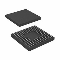
ADSP-BF531SBBC400 Analog Devices Inc, ADSP-BF531SBBC400 Datasheet - Page 9

ADSP-BF531SBBC400
Manufacturer Part Number
ADSP-BF531SBBC400
Description
IC,MICROPROCESSOR,32-BIT,CMOS,BGA,160PIN,PLASTIC
Manufacturer
Analog Devices Inc
Series
Blackfin®r
Type
Fixed Pointr
Datasheet
1.ADSP-BF531SBSTZ400.pdf
(12 pages)
Specifications of ADSP-BF531SBBC400
Rohs Status
RoHS non-compliant
Interface
SPI, SSP, UART
Clock Rate
400MHz
Non-volatile Memory
ROM (1 kB)
On-chip Ram
52kB
Voltage - I/o
1.8V, 2.5V, 3.3V
Voltage - Core
1.20V
Operating Temperature
-40°C ~ 85°C
Mounting Type
Surface Mount
Package / Case
160-CSPBGA
Device Core Size
16b
Architecture
Modified Harvard
Format
Fixed Point
Clock Freq (max)
400MHz
Mips
400
Device Input Clock Speed
400MHz
Operating Supply Voltage (typ)
1.2/1.8/2.5/3.3V
Operating Supply Voltage (min)
0.8/1.75V
Operating Supply Voltage (max)
1.32/3.6V
Operating Temp Range
-40C to 85C
Operating Temperature Classification
Industrial
Mounting
Surface Mount
Pin Count
160
Package Type
CSPBGA
Package
160CSP-BGA
Numeric And Arithmetic Format
Fixed-Point
Maximum Speed
400 MHz
Device Million Instructions Per Second
400 MIPS
For Use With
ADZS-BF533-EZLITE - KIT W/BOARD EVAL FOR ADSP-BF533
Lead Free Status / Rohs Status
Not Compliant
Available stocks
Company
Part Number
Manufacturer
Quantity
Price
Company:
Part Number:
ADSP-BF531SBBC400
Manufacturer:
ADI
Quantity:
329
Company:
Part Number:
ADSP-BF531SBBC400
Manufacturer:
Analog Devices Inc
Quantity:
10 000
Part Number:
ADSP-BF531SBBC400
Manufacturer:
ADI/亚德诺
Quantity:
20 000
Silicon Anomaly List
11.
12.
DESCRIPTION:
For certain PPI configurations, the general-purpose timers can be utilized as frame sync signals. When the PPI is set up for transmit modes
that utilize one or more external frame syncs, the general-purpose timers will have limited functionality.
WORKAROUND:
The anomaly only applies to the "PPI transmit with 2 external frame syncs" mode, and only the TMR2 pin is affected. Timer 2 must be
enabled and is not available for general use.
APPLIES TO REVISION(S):
0.3
DESCRIPTION:
A false Code or Data Protection Exception may be raised if it is caused by a speculative fetch that is cancelled. For instance, if a jump or an
rts instruction located at the last word of a valid page branches to another valid page, but the speculative instruction fetch was from an
invalid or non-existing memory location, an exception would still be raised. Similarly, if a post-incremented indirect data memory access
performs a speculative access to a protected or non-existing memory location (for instance R0 = [P0++]; where P0 points to the last word
of a page) an incorrect exception would occur.
WORKAROUND:
1) Do not place branch instructions or data at page boundaries. Leave at least 76 bytes free before any boundary with a reserved memory
space. This will prevent false exceptions from occuring.
2) Have the exception handler confirm whether the exception was valid or not before taking action. This can be done by verifying if the
CODE_FAULT_ADDR (or the DATA_FAULT_ADDR) register contains an address that is within a valid page. In that case, no action is
performed.
The default VisualDSP++ LDFs include a workaround for this hardware anomaly. The workaround will be automatically enabled for the
appropriate silicon revisions, or the workaround can be enabled manually by defining the macro
__WORKAROUND_AVOID_LDF_BLOCK_BOUNDARIES when linking.
When enabled, the LDFs will reserve 76 bytes at the boundaries of valid memory blocks.
APPLIES TO REVISION(S):
0.3
05000183 - Timer Pin Limitations for PPI TX Modes with External Frame Syncs:
05000189 - False Protection Exceptions when Speculative Fetch Is Cancelled:
NR003532D | Page 9 of 45 | July 2008
ADSP-BF531/BF532/BF533


