ADUC7060BSTZ32 Analog Devices Inc, ADUC7060BSTZ32 Datasheet - Page 2
ADUC7060BSTZ32
Manufacturer Part Number
ADUC7060BSTZ32
Description
DUAL 24-BIT AFE AND ARM 7 I.C
Manufacturer
Analog Devices Inc
Series
MicroConverter® ADuC7xxxr
Specifications of ADUC7060BSTZ32
Design Resources
4 mA-to-20 mA Loop-Powered Temperature Monitor Using ADuC7060/1 (CN0145) Low power, Long Range, ISM Wireless Measuring Node (CN0164)
Core Processor
ARM7
Core Size
16/32-Bit
Speed
10MHz
Connectivity
I²C, SPI, UART/USART
Peripherals
POR, PWM, Temp Sensor, WDT
Number Of I /o
14
Program Memory Size
32KB (16K x 16)
Program Memory Type
FLASH
Ram Size
4K x 8
Voltage - Supply (vcc/vdd)
2.375 V ~ 2.625 V
Data Converters
A/D 5x24b, 8x24b, D/A 1x14b
Oscillator Type
Internal
Operating Temperature
-40°C ~ 125°C
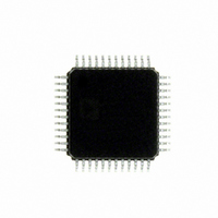
Package / Case
48-LQFP
Cpu Family
ADuC7xxx
Device Core
ARM7TDMI
Device Core Size
16/32Bit
Frequency (max)
10.24MHz
Interface Type
I2C/SPI/UART
Total Internal Ram Size
4KB
# I/os (max)
14
Number Of Timers - General Purpose
4
Operating Supply Voltage (typ)
2.5V
Operating Supply Voltage (max)
2.625V
Operating Supply Voltage (min)
2.375V
On-chip Adc
2(4-chx24-bit)
Instruction Set Architecture
RISC
Operating Temp Range
-40C to 125C
Operating Temperature Classification
Automotive
Mounting
Surface Mount
Pin Count
48
Package Type
LQFP
Package
48LQFP
Family Name
ADuC7xxx
Maximum Speed
10.24 MHz
Operating Supply Voltage
2.5 V
Data Bus Width
16|32 Bit
Number Of Programmable I/os
14
Number Of Timers
4
Lead Free Status / RoHS Status
Lead free / RoHS Compliant
Eeprom Size
-
Lead Free Status / Rohs Status
Compliant
Available stocks
Company
Part Number
Manufacturer
Quantity
Price
Company:

Part Number:
ADUC7060BSTZ32
Manufacturer:
CYPRESS
Quantity:
294
Company:
Part Number:
ADUC7060BSTZ32
Manufacturer:
ADI
Quantity:
315
Company:
Part Number:
ADUC7060BSTZ32
Manufacturer:
Analog Devices Inc
Quantity:
10 000
Part Number:
ADUC7060BSTZ32
Manufacturer:
ADI/亚德诺
Quantity:
20 000
Company:
Part Number:
ADUC7060BSTZ32-RL
Manufacturer:
Analog Devices Inc
Quantity:
10 000


ADuC7060/ADuC7061
TABLE OF CONTENTS
Features .............................................................................................. 1
Applications....................................................................................... 1
General Description ......................................................................... 1
Revision History ............................................................................... 3
Functional Block Diagram .............................................................. 4
Specifications..................................................................................... 5
Absolute Maximum Ratings.......................................................... 14
Pin Configurations and Function Descriptions ......................... 15
Terminology .................................................................................... 20
Overview of the ARM7TDMI Core............................................. 21
Oscillator, PLL, and Power Control ............................................. 34
ADC Circuit Information.............................................................. 38
DAC Peripherals ............................................................................. 56
Electrical Specifications............................................................... 5
Timing Specifications ................................................................ 10
ESD Caution................................................................................ 14
Thumb Mode (T)........................................................................ 21
Multiplier (M) ............................................................................. 21
EmbeddedICE (I) ....................................................................... 21
ARM Registers ............................................................................ 21
Interrupt Latency........................................................................ 22
Memory Organization ............................................................... 22
Flash/EE Control Interface........................................................ 23
Memory Mapped Registers ....................................................... 27
Complete MMR Listing............................................................. 28
Reset ............................................................................................. 33
Clocking System ......................................................................... 34
Power Control System................................................................ 34
Reference Sources....................................................................... 39
Diagnostic Current Sources ...................................................... 39
Sinc3 Filter................................................................................... 40
ADC Chopping........................................................................... 40
Programmable Gain Amplifier................................................. 40
Excitation Sources ...................................................................... 40
ADC Low Power Mode.............................................................. 40
ADC Comparator and Accumulator ....................................... 41
Temperature Sensor ................................................................... 41
ADC MMR Interface ................................................................. 41
Example Application Circuits................................................... 54
DAC.............................................................................................. 56
Rev. C | Page 2 of 108
Nonvolatile Flash/EE Memory ..................................................... 58
Processor Reference Peripherals................................................... 59
Timers .............................................................................................. 66
Pulse-Width Modulator................................................................. 75
UART Serial Interface .................................................................... 80
I
Serial Peripheral Interface ............................................................. 96
General-Purpose I/O ................................................................... 101
2
C ..................................................................................................... 86
MMR Interface ........................................................................... 56
Using the DAC............................................................................ 57
Flash/EE Memory Reliability.................................................... 58
Programming.............................................................................. 58
Interrupt System ......................................................................... 59
IRQ ............................................................................................... 59
Fast Interrupt Request (FIQ) .................................................... 60
Programmed Interrupts............................................................. 61
Vectored Interrupt Controller (VIC)....................................... 61
VIC MMRs.................................................................................. 61
Timer0.......................................................................................... 67
Timer1 or Wake-Up Timer ....................................................... 69
Timer2 or Watchdog Timer ...................................................... 71
Timer3.......................................................................................... 73
Pulse-Width Modulator General Overview ........................... 75
Baud Rate Generation................................................................ 80
UART Register Definitions ....................................................... 80
Configuring External Pins for I
Serial Clock Generation ............................................................ 87
I
I
MISO (Master In, Slave Out) Pin............................................. 96
MOSI (Master Out, Slave In) Pin............................................. 96
SCLK (Serial Clock I/O) Pin..................................................... 96
Slave Select (P0.0/ SS ) Input Pin ............................................... 96
Configuring External Pins for SPI Functionality................... 96
SPI Registers................................................................................ 97
GPxCON Registers................................................................... 101
GPxDAT Registers ................................................................... 102
GPxSET Registers..................................................................... 102
GPxCLR Registers.................................................................... 102
GPxPAR Registers .................................................................... 102
2
2
C Bus Addresses....................................................................... 87
C Registers ................................................................................ 87
2
C Functionality ................... 86
Related parts for ADUC7060BSTZ32
Image
Part Number
Description
Manufacturer
Datasheet
Request
R

Part Number:
Description:
±1.7g Dual-Axis IMEMS Accelerometer Evaluation Board
Manufacturer:
Analog Devices Inc
Datasheet:

Part Number:
Description:
Inertial Sensor Evaluation System
Manufacturer:
Analog Devices Inc
Datasheet:
Part Number:
Description:
Manufacturer:
Analog Devices Inc
Datasheet:
Part Number:
Description:
Manufacturer:
Analog Devices Inc
Datasheet:
Part Number:
Description:
Manufacturer:
Analog Devices Inc
Datasheet:
Part Number:
Description:
Manufacturer:
Analog Devices Inc
Datasheet:
Part Number:
Description:
Manufacturer:
Analog Devices Inc
Datasheet:
Part Number:
Description:
Manufacturer:
Analog Devices Inc
Datasheet:
Part Number:
Description:
Manufacturer:
Analog Devices Inc
Datasheet:
Part Number:
Description:
Manufacturer:
Analog Devices Inc
Datasheet:
Part Number:
Description:
Manufacturer:
Analog Devices Inc
Datasheet:
Part Number:
Description:
Manufacturer:
Analog Devices Inc
Datasheet:
Part Number:
Description:
Manufacturer:
Analog Devices Inc
Datasheet: