ADXL322EB Analog Devices Inc, ADXL322EB Datasheet
ADXL322EB
Specifications of ADXL322EB


Related parts for ADXL322EB


ADXL322EB Summary of contents
Page 1
FEATURES Small and thin 4 mm × × 1.45 mm LFCSP package 2 mg resolution Wide supply voltage range: 2 Low power: 340 μ 2.4 V (typ) S ...
Page 2
ADXL322 TABLE OF CONTENTS Specifications..................................................................................... 3 Absolute Maximum Ratings............................................................ 4 ESD Caution.................................................................................. 4 Pin Configuration and Function Descriptions............................. 5 Typical Performance Characteristics (V Theory of Operation ...................................................................... 11 Performance ................................................................................ 11 Applications..................................................................................... 12 Power Supply Decoupling ......................................................... 12 REVISION HISTORY ...
Page 3
SPECIFICATIONS T = 25° 0.1 μF, Acceleration = 0 g, unless otherwise noted Table 1. Parameter SENSOR INPUT Measurement Range Nonlinearity Package Alignment Error Alignment Error Cross-Axis Sensitivity ...
Page 4
ADXL322 ABSOLUTE MAXIMUM RATINGS Table 2. Parameter Acceleration (Any Axis, Unpowered) Acceleration (Any Axis, Powered All Other Pins Output Short-Circuit Duration (Any Pin to Common) Operating Temperature Range Storage Temperature ESD CAUTION ESD (electrostatic discharge) sensitive device. Electrostatic ...
Page 5
PIN CONFIGURATION AND FUNCTION DESCRIPTIONS Table 3. Pin Function Descriptions Pin No. Mnemonic COM COM 6 COM 7 COM OUT OUT 13 ...
Page 6
ADXL322 Table 4. Recommended Soldering Profile Profile Feature Average Ramp Rate ( Preheat Minimum Temperature (T ) SMIN Minimum Temperature (T ) SMAX Time ( SMIN SMAX ...
Page 7
TYPICAL PERFORMANCE CHARACTERISTICS ( 1.40 1.42 1.44 1.46 1.48 1.50 1.52 1.54 1.56 1.58 1.60 OUTPUT (V) Figure 5. X-Axis Zero g Bias at 25° ...
Page 8
ADXL322 1.600 1.575 1.550 1.525 1.500 1.475 1.450 1.425 1.400 –40 – TEMPERATURE (°C) Figure 11. Zero g Bias vs. Temperature—Parts Soldered to PCB 150 160 170 180 190 ...
Page 9
SELF-TEST (V) Figure 17. X-Axis Self-Test Response at 25° 350 370 390 410 430 450 470 CURRENT ( μ A) ...
Page 10
ADXL322 X = 1.50V OUT Y = 1.92V OUT 1.08V OUT 322J #1234 Y = 1.50V OUT 5678P X = 1.50V OUT Y = 1.08V OUT 5678P X = 1.92V OUT #1234 322J Y = 1.50V OUT ...
Page 11
THEORY OF OPERATION The ADXL322 is a complete acceleration measurement system on a single monolithic IC. The ADXL322 has a measurement range of ± contains a polysilicon surface micromachined sensor and signal conditioning circuitry to implement an open- ...
Page 12
ADXL322 APPLICATIONS POWER SUPPLY DECOUPLING For most applications, a single 0.1 μF capacitor, C decouples the accelerometer from noise on the power supply. However, in some cases, particularly where noise is present at the 140 kHz internal clock frequency (or ...
Page 13
Peak-to-peak noise values give the best estimate of the uncer- tainty in a single measurement. Table 7 gives the typical noise output of the ADXL322 for various C and C X Table 7. Filter Capacitor Selection (C X Bandwidth C ...
Page 14
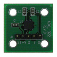
... ADXL322 OUTLINE DIMENSIONS PIN 1 INDICATOR 1.50 1.45 1.40 ORDERING GUIDE Measurement Model Range 1 ADXL322JCP ± ADXL322JCP–REEL ±2 g ADXL322EB 1 Lead finish—Matte tin. 0.20 MIN 12 4.15 TOP 4.00 SQ VIEW 3.85 0.65 BSC 9 0.55 0.50 0.45 0.05 MAX 0.02 NOM 0.35 COPLANARITY ...
Page 15
NOTES Rev Page ADXL322 ...
Page 16
ADXL322 NOTES © 2007 Analog Devices, Inc. All rights reserved. Trademarks and registered trademarks are the property of their respective owners. D05589–0–6/07(0) Rev Page ...